Cortex-M3 core at 50 MHz with on-chip memory budget
The LM3S1538-EQC50-A2: That clock rate, combined with the single-cycle multiply and hardware divide in the Cortex-M3 pipeline, delivers deterministic interrupt response for time-constrained control loops. On-chip memory totals 96 KB of Flash for program storage and 64 KB of SRAM for data — a 1.5:1 Flash-to-RAM ratio that suits firmware with moderate lookup tables or buffering. The 64 KB SRAM is mapped as 64K x 8, giving the linker a contiguous data space without banking. Operating temperature spans -40°C to +105°C, which qualifies the part for industrial enclosures, motor-drive compartments, and outdoor telecom cabinets where ambient heat rises above the commercial 85°C ceiling.
The MCU integrates 43 general-purpose I/O lines and a peripheral set that includes I²C, SPI, SSI, UART/USART, IrDA, Microwire, and QEI (quadrature encoder interface). The QEI block directly decodes incremental encoder pulses for motor position feedback without bit-banging the timer. On-chip analog conversion is handled by an 8-channel, 10-bit ADC — sufficient for monitoring analog sensors or current-sense resistors in a single-ended configuration. Supervisory functions include brown-out detect, power-on reset, a watchdog timer, and a PWM module — the brown-out reset holds the core in reset until the supply rail stabilises above the threshold, preventing code execution during a sag.
Package, supply, and board-fit constraints
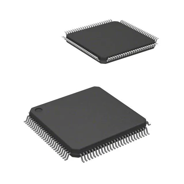
Housed in a 100-pin LQFP with a 14x14 mm body (0.50 mm pitch), the LM3S1538-EQC50-A2 requires a 4-layer PCB for reliable fan-out of the inner rows. The 100-LQFP footprint is shared across several Stellaris 1000-series devices, so a single PCB layout can accommodate multiple Flash/RAM variants by populating the matching BOM line — useful for a product family with tiered firmware requirements.
Texas Instruments has marked the LM3S1538-EQC50-A2 as obsolete.