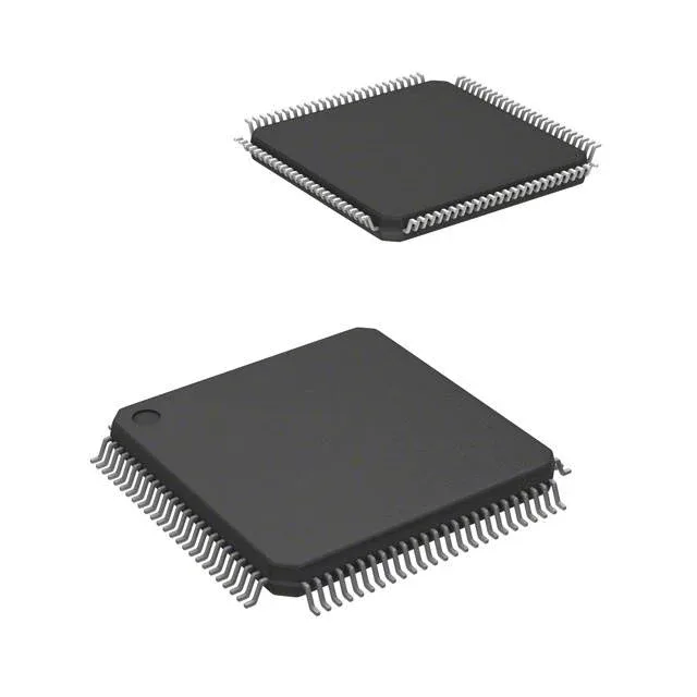
Texas Instruments has marked the LM3S1138-IQC50-A2T as Obsolete. The 100-LQFP footprint and 2.25–2.75 V supply rail mean a pin-compatible replacement would need to match both the package and the non-standard voltage domain.
Memory and peripheral budget for the BOM line
The 64 KB on-chip Flash and 16 KB SRAM set the application ceiling — a firmware image with a full HAL and RTOS stack leaves roughly 20–30 KB free for the application layer, depending on the peripheral driver footprint. The 46 GPIOs cover most sensor and actuator interfaces without external port expansion. Connectivity includes I²C, SPI, SSI, UART/USART, and IrDA — the Microwire and SSI modes are legacy synchronous protocols that share pins with the SPI module, so a design using both SPI and SSI simultaneously must check the pin mux table.
This is narrower than the common 3.3 V MCU supply; a board already running 3.3 V needs a separate LDO or a buck converter for this part. The internal oscillator saves a crystal on the BOM for applications that tolerate ±2–3% clock accuracy over temperature.
ADC and analog front-end
Eight 10-bit ADC channels sample at up to 1 MSps typical — sufficient for reading thermistor arrays, potentiometer feedback, or current-sense amplifier outputs at control-loop rates below 100 kHz per channel. The 10-bit resolution yields 1024 counts across the reference voltage; for a 2.5 V reference, each LSB represents roughly 2.44 mV. Brown-out detect and POR reset the core if the supply dips below the threshold, which matters for battery-powered or capacitor-backed applications where the rail decays slowly.
A 4-layer PCB is recommended for fan-out — the inner rows of the QFP require vias to escape, and the 2.25–2.75 V core rail benefits from a dedicated power plane. The exposed pad on the LQFP-100 is not present; thermal dissipation relies on the leadframe and the board copper under the package body. Surface-mount reflow follows standard JEDEC MSL ratings — confirm the moisture sensitivity level on the reel label before baking.