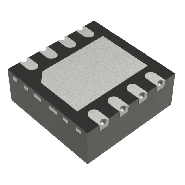
The LM393LVDSGR: Maximum quiescent current is 35 µA per device. For a battery-powered sensor node that wakes periodically to compare a thermistor or photodiode threshold, the comparator's own draw sits well below the microcontroller's sleep current — the system's idle power is dominated by the sensor bias, not the comparator.
Propagation delay and input bias — speed versus source impedance
600 ns maximum propagation delay sets the response ceiling for overcurrent or zero-crossing detection — at a 1 MHz clock rate the delay is less than one cycle, but at 10 MHz the comparator's output lags by six cycles, so it is best suited for sub-MHz threshold events rather than high-speed data recovery. Maximum input bias current is 5 pA at 5 V. With a 10 MΩ source impedance the voltage error is 50 µV — negligible for most window comparators, but a 100 MΩ piezoelectric sensor would see a 500 µV offset that shifts the threshold by half the input offset spec. The 2 mV maximum input offset voltage is the dominant error term for low-impedance sources.
Open-drain output and package — wired-OR and board area
Open-drain output lets multiple comparators share a common pull-up resistor for wired-OR logic — a single interrupt line from several over-temperature or over-current detectors collapses to one GPIO pin without external logic gates. The 8-WSON package (2x2 mm,) with exposed thermal pad fits into a 2-layer board where the pad is soldered to a ground-plane via array — the thermal resistance drops by roughly 40% compared to a non-pad SOIC, keeping the junction below 125°C even when sinking 100 mA from the output into a short circuit.
Temperature grade and noise rejection
An engine-bay ECU that sees 105°C on a summer day still has 20°C of margin before the absolute-maximum junction rating is reached. Typical CMRR is 65 dB and PSRR is 80 dB. At 65 dB CMRR, a 1 V common-mode shift at the input appears as a 560 µV offset at the output — well within the 2 mV input offset spec, so the threshold stays stable across ground shifts in a noisy backplane.