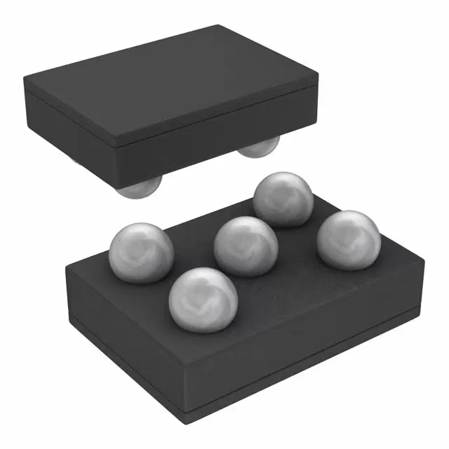
350 mA buck in a 1.41 x 1.08 mm DSBGA
The LM3673TL-ADJ/NOPB: The output is adjustable from 1.1 V up to 3.3 V, set by an external resistor divider. It uses a synchronous rectifier — the internal low-side FET replaces the external Schottky diode, saving board area and improving efficiency at light loads.
Package reality: 5-bump DSBGA
Housed in a 5-WFBGA, DSBGA (supplier device package 5-DSBGA, 1.41 x 1.08 mm), this is a wafer-level chip-scale package. The 0.5 mm bump pitch demands a controlled SMT process — the board land pattern must match TI's recommended stencil aperture to avoid solder bridging. Operating temperature range is -30 °C to 85 °C ambient, covering most industrial and consumer environments but not extended automotive or high-temp applications. Cut Tape works for prototype or low-volume builds.