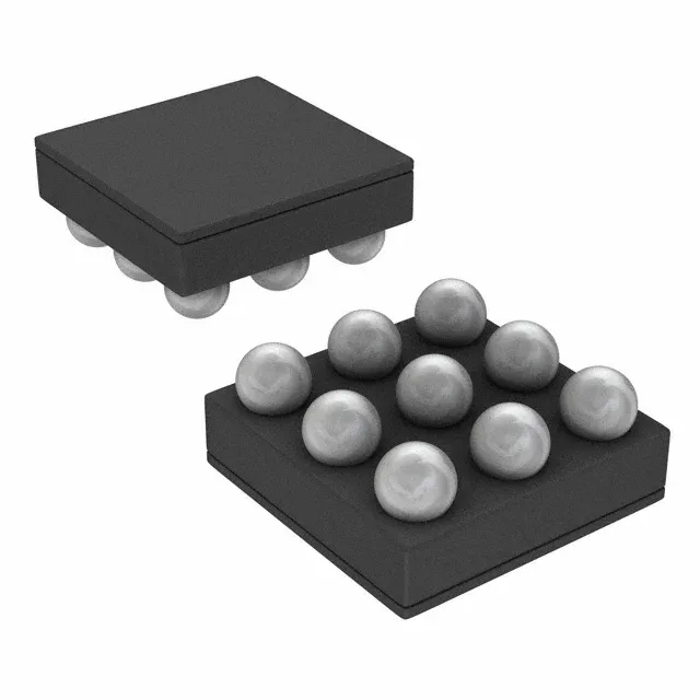
Boost regulator for camera flash — what the 1.5 A rating means
The LM3642TLX-LT/NOPB is a single-channel DC-DC boost regulator from Texas Instruments, purpose-built for camera flash LED drive. Its 1.5 A flash current is the peak the internal switch delivers during the strobe; the 4 MHz switching frequency keeps the inductor and output capacitor small enough for a phone- or module-level board. The part integrates the switch, so the BOM stays to one inductor and a few ceramics — no external FET. Dimming is handled over I²C, which means the host processor sets the flash current and timing in register writes, not a PWM pin.
Package reality — 9-DSBGA and what it demands from layout
Housed in a 9-bump DSBGA measuring 1.6 × 1.6 mm, the LM3642TLX-LT/NOPB is a wafer-level chip-scale package. The 0.5 mm bump pitch is standard for this form factor, but the board-side solder mask opening and via-in-pad strategy must match the TI land pattern — a 2-layer board with microvias under the bumps is typical.
Active lifecycle and compliance paperwork
The 5 V output is the regulated boost rail feeding the LED anode; the cathode connects through the sense resistor back to the part.