SEPIC topology — why it matters for battery-powered backlights
The LM3410XSD/NOPB is a DC-DC regulator supporting both SEPIC and step-up (boost) topologies. The SEPIC capability is the key differentiator here: it can regulate an output voltage above, below, or equal to the input voltage using a single inductor and a coupling capacitor. For a backlight driver running from a Li-Ion battery (3.0-4.2 V), the LED string voltage may be 9 V (three series LEDs) or 6 V (two series LEDs), and the battery voltage crosses the LED string voltage during discharge. A standard boost converter would drop out of regulation when the battery voltage exceeds the LED string voltage; the SEPIC topology keeps the LEDs lit across the full battery range.
2.8 A switch current — the power-stage ceiling, not the LED current
The 2.8 A rating is the peak current the internal N-channel switch can handle, not the continuous LED current. The actual LED current is set by the external sense resistor and the inductor ripple current.
PWM dimming — logic-level control, not analog
Dimming is controlled by a PWM signal applied to the shutdown or feedback pin, not by an analog voltage on a dedicated dimming pin. The PWM frequency should be above 200 Hz to avoid visible flicker, and the minimum on-time of the internal switch (typically 100-200 ns) sets the minimum dimming pulse width. At a 1.6 MHz switching frequency, the PWM dimming ratio is limited by the switching cycle time — a 1% duty cycle at 200 Hz PWM is 50 µs, which is 80 switching cycles, enough for the inductor current to settle. The output voltage range of 3 V to 24 V means the part can drive up to six white LEDs in series at 3.3 V each, or a single high-voltage LED string.
Temperature grade and package — board-fit checklist
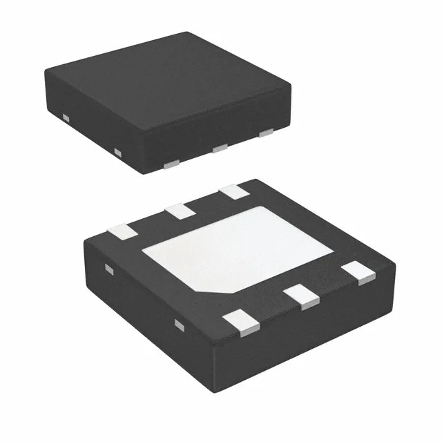
The operating junction temperature range is -40°C to 125°C, which covers automotive under-hood and industrial environments. The recommended land pattern from TI includes a 2.2x2.2 mm pad with four thermal vias (0.3 mm diameter) to the ground plane. The narrow leads (0.4 mm pitch) require a solder paste stencil thickness of 0.125 mm to avoid bridging. The part is ROHS3 compliant (no RoHS exemptions), so it is fully lead-free and suitable for EU-market products without an exemption expiry date.
Sourcing and compliance documentation
Texas Instruments provides the LM3410XSD/NOPB with full compliance documentation: ROHS3 certification (no exemption-based RoHS), REACH compliance data, and the standard TI product change notification (PCN) process.