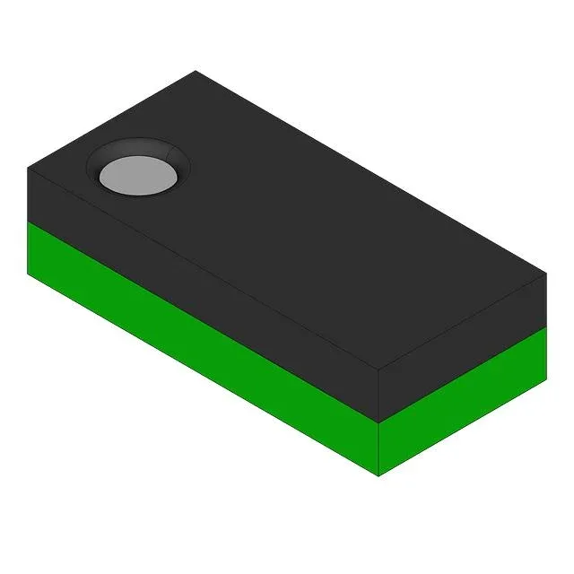
Step-down regulator in a 2x1.3 mm DSBGA
The LM3205TL/NOPB is a 650 mA adjustable step-down (buck) converter from Texas Instruments, switching at 2 MHz and packaged in an 8-bump DSBGA measuring 2x1.3 mm. The synchronous rectifier eliminates the external Schottky diode, saving board area and improving efficiency at light loads — a practical advantage when every mm² counts in a wearable or IoT node.
Switching frequency and thermal envelope
Operating temperature spans -30 °C to 85 °C — this is the commercial/industrial band, not automotive. The DSBGA's thermal resistance depends heavily on PCB copper area; the 650 mA rating assumes adequate board-level heat spreading. At 650 mA continuous output, the internal switch's Rds(on) at junction temperature determines the conduction loss — the 2 MHz switching adds AC losses from gate charge and output capacitance, so the total efficiency peaks in the 200-400 mA range for typical 3.3 V to 1.8 V conversions.
The 8-WFBGA, DSBGA package with a 2x1.3 mm footprint is a wafer-level chip-scale package — the bumps are the I/O. The 0.5 mm pitch demands a PCB with at least two layers for fan-out; the centre bump is the thermal pad and should be stitched to the ground plane with multiple vias.
Lifecycle and compliance
As a TI-branded device, the datasheet, application notes, and IBIS models are available from the manufacturer's product page.