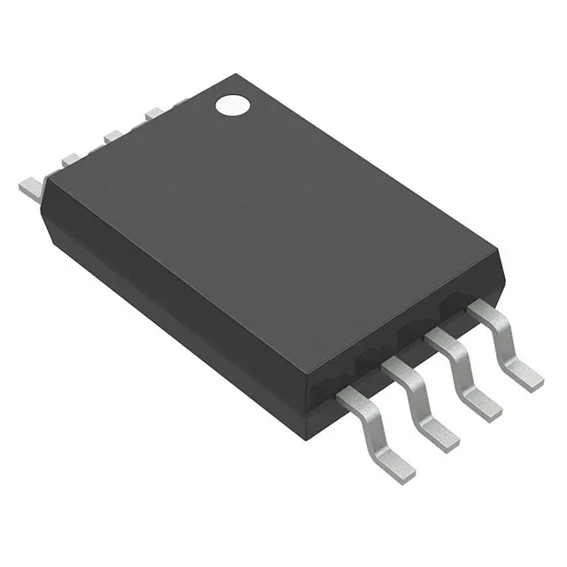
LM2904BQPWRQ1

Texas Instruments

Texas Instruments LM2904BQPWRQ1, Automotive Grade dual general-purpose operational amplifier, 1.2 MHz gain-bandwidth, 0.5 V/µs slew rate, 3 V to 36 V supply, 300 µA per channel, -40°C to 125°C, 8-TSSOP package, AEC-Q100 qualified.

Texas Instruments LM2904BQPWRQ1
Download datasheet (PDF)
[IN STOCK] In Stock: 1,000 pcs
$0.76/ pc

Volume pricing

Buy Now

MOQ 1 · Tape & Reel (TR) Cut Tape (CT) · RoHS · EIA-481 · DAP/DDP · T/T

Technical specifications

LM2904BQPWRQ1 specifications
Parameter / AttributeSpecification / Value
MountingSurface Mount
Amplifier typeGeneral Purpose
Voltage - input offset1 mV
Voltage - supply span36 V
Current - supply300µA (x2 Channels)
Current - input bias10 nA
Current - output (Channel)30 mA
Operating temperature-40°C ~ 125°C (TA)
Gain bandwidth product1.2 MHz
GradeAutomotive
PackageTape & Reel (TR) Cut Tape (CT)
Slew rate0.5V/µs
QualificationAEC-Q100
Case8-TSSOP (0.173\", 4.40mm Width)
Number of circuits2
100% Footprint Match · Solder-Ready (No PCB Redesign Needed)

Need Stock or a Drop-in Second-Source for LM2904BQPWRQ1?

Package: SOIC-8 · Pin-compatible replacements with immediate Shenzhen spot stock

Footprint Match 100%
Supply Chain & Allocation Reality:

The ubiquitous dual op-amp designed in the 1970s. While cheap, legacy bipolar LM358 parts suffer from crossover distortion and output swing limited to V+ - 1.5V. Modern precision drop-in replacements like SGMicro SGM8552 and 3PEAK TP358 deliver rail-to-rail I/O, lower offset voltage, and microamp quiescent power at comparable pricing.

Verified Pin-Compatible Replacements (2 verified alternatives)

SGM8552-SR SGMicro SOIC-8
100% Drop-in (Zero Code Change)
Availability & Target Pricing:

Rail-to-Rail Performance with High Dynamic Range ADC Support

Shenzhen Spot Inventory (24h Dispatch)

Electrical & Core Specs:

1.5 MHz Gain Bandwidth, Rail-to-Rail Input and Output

2.5V – 5.5V single supply (or ±1.25V to ±2.75V dual)

Compatibility & Drop-In Notes: No firmware interaction. Analog signal conditioning drop-in.
Package & Solder Footprint: Direct pin-for-pin replacement in SOIC-8 / MSOP-8. Rail-to-rail output swing allows full 0V to 3.3V / 5.0V ADC dynamic range utilization without losing 1.5V overhead.
Shenzhen Warehouse Stock & MOQ: SGMicro is China premier precision analog IC manufacturer; Tier-1 automotive and mobile OEM approved.
TP358-SR 3PEAK SOIC-8
100% Drop-in (Zero Code Change)
Availability & Target Pricing:

Large Factory Buffer Stock & Zero Allocation Risk

Large Factory Buffer Stock

Electrical & Core Specs:

1.0 MHz GBW, Low Quiescent Current (60 µA/ch)

2.1V – 5.5V single supply

Compatibility & Drop-In Notes: None.
Package & Solder Footprint: Direct solder drop-in on standard SOIC-8 op-amp layout.
Shenzhen Warehouse Stock & MOQ: Zero allocation risk; full factory COC and batch reel traceability.
Buyer & Quality Checklist for Sourcing Alternatives
  • Check maximum supply voltage: legacy bipolar LM358 operates up to 32V; if your circuit runs on 12V–24V supply rails, select high-voltage variants (e.g., SGM8272 or TP156) instead of 5.5V rail-to-rail models.
  • Confirm ADC input scaling: rail-to-rail output swings up to VCC - 10mV, allowing higher dynamic measurement resolution for current sense shunts.
Frequently Asked Technical Questions

Q: When should I upgrade from legacy LM358 to SGM8552 or TP358?

A: Upgrade if your system operates on 3.3V or 5V logic rails and feeds an internal microcontroller ADC. Legacy LM358 cannot drive outputs higher than ~1.8V on a 3.3V supply, throwing away nearly half of your ADC conversion resolution. Rail-to-rail alternatives solve this instantly with zero board changes.

Technical details

The supply span from 3 V to 36 V covers both 12 V passenger-car and 24 V truck electrical systems without requiring a separate regulator. Each of the two channels draws 300 µA typical supply current, which keeps the quiescent load low for always-on electronic control units.

Input offset and bias — what to budget in production

For a production design, these are the limits to use in worst-case error budgeting rather than relying on typical values. In a high-gain sensor amplifier, the 1 mV offset translates to a DC error at the output that must be accounted for in the system calibration routine or trimmed during end-of-line test. For loads above 30 mA, buffer the output with a transistor stage.

Package and footprint — 8-TSSOP

The 0.65 mm pin pitch is standard for this package family; verify the land pattern against the IPC-7351B nominal footprint before layout. No exposed thermal pad — junction-to-ambient thermal resistance is managed through the PCB copper area.

It is ROHS3 compliant.

LM2904BQPWRQ1
[ALLOC] verified
Quote