Boost converter with a 2.55A switch — sizing the output current
The LM2700LD-ADJ/NOPB is a current-mode step-up (boost) regulator from Texas Instruments, built around a 2.55 A internal switch.
Dual switching frequency — 600 kHz or 1.25 MHz
The part switches at either 600 kHz or 1.25 MHz, selected via a single resistor to ground. At 1.25 MHz the inductor and output capacitor shrink — a 4.7 µH inductor and 10 µF ceramic output cap are typical — but switching losses in the internal NPN switch rise, so efficiency drops a few points at light load. At 600 kHz the inductor is roughly twice the value, but the efficiency curve peaks higher, especially above 50% load. The trade-off is between board area and thermal budget. No synchronous rectifier is used — the external Schottky diode (e.g., a 3 A, 20 V part) handles the catch current. The diode's forward drop and reverse recovery add to the loss; a low-Vf Schottky keeps the efficiency above 85% in the mid-load range. The diode selection directly affects the output ripple and the switch voltage stress during the off-time.
Input and output voltage range — where it fits
The adjustable output goes from a 1.26 V reference up to 17.5 V — that covers 12 V rails, 15 V bias lines, and OLED/VFD supplies. The 17.5 V maximum is set by the switch breakdown, not the feedback divider; keep the output below that to avoid avalanche stress on the switch.
Package and thermal — the exposed pad is the heatsink
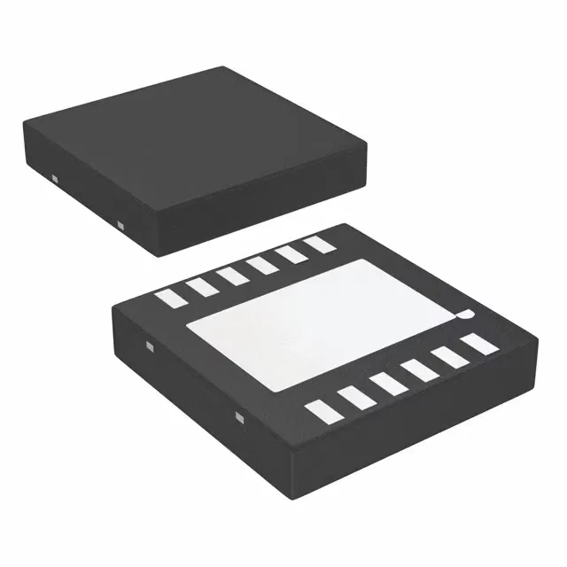
The 14-WFDFN with exposed pad (4x4 mm WSON) routes the thermal path through the die attach pad. Solder the pad to a copper plane on the top layer and use vias to a ground plane on the inner or bottom layer — the datasheet recommends a 1 in² copper area for full 2.55 A switch operation at high ambient. Without that thermal relief, the junction temperature climbs above the 125 °C absolute maximum under sustained heavy load.