What the AEC-Q100 grade means for your automotive power rail
The LM2623QNHLTQ1: The 0.9V minimum input voltage lets it start from a single-cell alkaline or Li-ion battery that has dropped to near-depletion, while the 14V maximum input and output handle the 12V nominal automotive bus with headroom for load-dump transients up to the abs-max rating of the internal switch.
Switching specs and the external diode trade-off
The internal switch is rated for 2.85A continuous — this is the peak inductor current the FET can sustain, not the output current. For a typical 5V output from a 3.3V rail, the maximum output current is roughly 1.5A before the switch current limit engages, assuming 90% efficiency and a properly sized inductor. The trade-off is that switching losses in the external Schottky diode (required because the part is non-synchronous) become a larger fraction of total loss at 2MHz than at 500kHz, so the diode must be rated for fast recovery (less than 10ns reverse recovery time) to avoid overheating. The adjustable output is set by a resistor divider from the 1.24V internal reference — the feedback pin draws less than 100nA, so divider resistors in the 10k-100k range keep the quiescent current low without noise pickup on the feedback trace.
Package, footprint, and thermal management
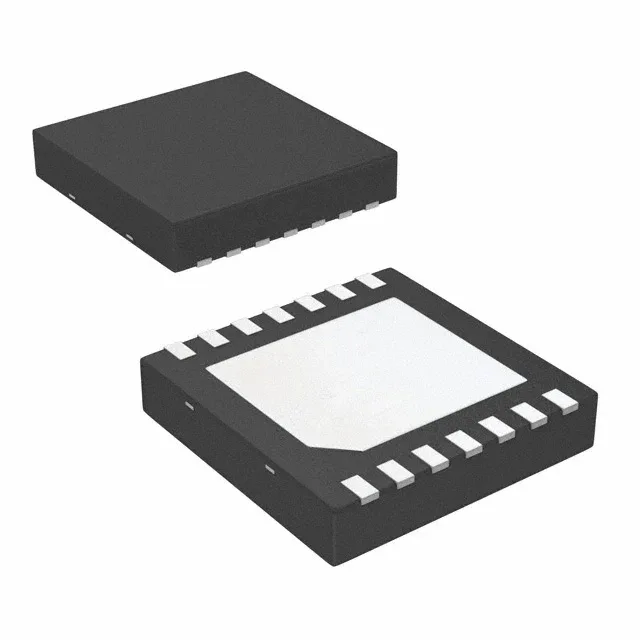
A 4-layer board with thermal vias under the pad is the standard layout — two-layer boards without a ground plane will see junction temperatures rise 15-20°C above the datasheet typical. The exposed pad is electrically connected to ground (the substrate of the IC), so the PCB copper plane under the pad is also the ground return for the input and output capacitors.
Active lifecycle and compliance documentation
No stock-holding claim is made; each RFQ is quoted fresh.