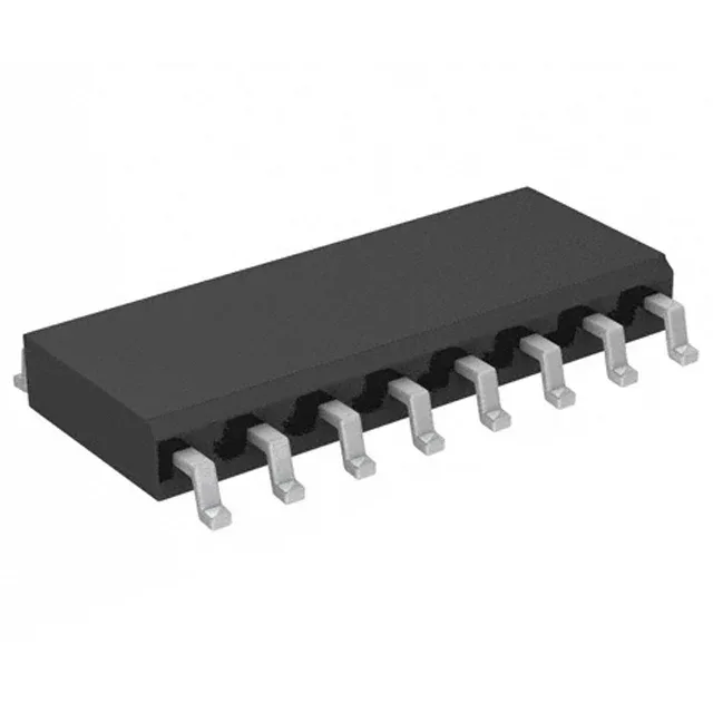
Quad LVDS receiver — what the 400 Mbps rating means for the backplane
With four independent receivers in one package, it handles a full 4-lane LVDS bus without external translation logic — common in camera-serializer links, FPGA-to-FPGA chip-to-chip interfaces, and high-speed backplane clock distribution. The 400 Mbps per-channel data rate (cite:) sets the signal-integrity budget: at that edge rate, stub lengths on the PCB must be kept under a few millimetres, and the differential pair impedance should be held to 100 Ω ±10% from driver to receiver input.
This does not mean an immediate end-of-life, but it signals that TI is no longer actively promoting this package variant for new socket wins. However, any new design-in should target the active sibling, the DS90LV048ATMX, which is the same die in a Tape & Reel package format — functionally identical, same 400 Mbps rating, same 16-SOIC footprint. The base product number DS90LV048 (cite:) covers both; the TM suffix indicates Tube, the TMX suffix indicates Tape & Reel. If your production line already handles Tape & Reel, the TMX variant is the straightforward BOM swap with no re-qualification needed.
Industrial temperature — rated for the factory floor
The LVDS common-mode input range of roughly 0 V to 2.4 V (typical for this family) means the receiver can tolerate a ground shift of a few hundred millivolts between driver and receiver, which is common in multi-box systems connected by a long cable.