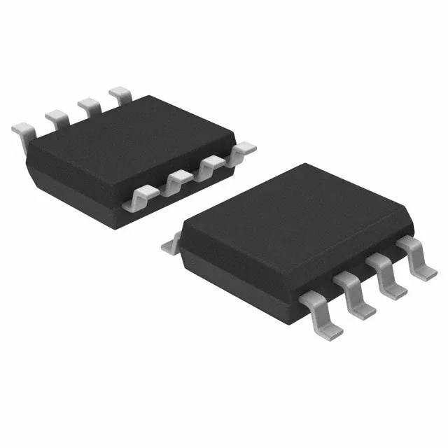
Signal-conditioning buffer for LVDS links
The DS90LV001TM: It accepts CML, LVDS, or LVPECL inputs and outputs a clean LVDS signal, making it a straightforward choice for extending trace length, fanning out clocks, or cleaning up a degraded eye diagram on a backplane or cable interconnect. Rated for a maximum data rate of 800 Mbps with a propagation delay of 1.4 ns, this part fits into the signal chain without adding significant latency — important for timing budgets in multi-drop or cascaded topologies.
Input flexibility reduces BOM risk
The DS90LV001TM accepts three common differential signaling standards on its input: CML, LVDS, and LVPECL. This means the same buffer can sit behind a SerDes output (CML), an FPGA differential I/O (LVDS), or a high-speed clock driver (LVPECL) without a level-shifting resistor network. For a BOM engineer, that reduces the number of unique signal-conditioning SKUs across a product family.
Route the differential pair in and out; decouple the supply with a capacitor near pin 8.