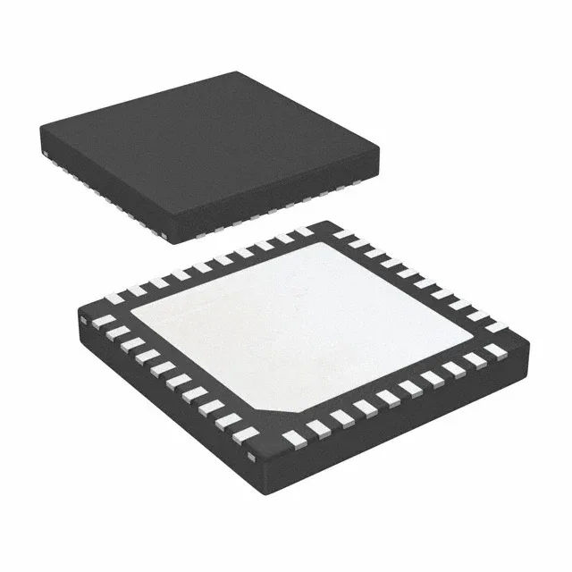
Texas Instruments DS10BR254TSQ/NOPB — Discrete Semiconductors

DS10BR254TSQ/NOPB LVDS Buffer Multiplexer, 1.5 Gbps, 40-WQFN

MPNDS10BR254TSQ/NOPB
End of Life

Texas Instruments DS10BR254TSQ/NOPB, LVDS Buffer/Multiplexer, 1 x 2:4, 1.5 Gbps max data rate, 440 ps delay, 3V-3.6V supply, -40 to 85°C, 40-WFQFN exposed pad, ROHS3 compliant.

$9.99Ref. price · indicative, final on quote
Packaging40-WFQFN Exposed Pad
StockContact for availability
MOQ1 pcs
  • 100% new & originalTraceable channels only — no refurbs, no pulls, no remarked parts.
  • Date & lot codes on quoteStated per line before you commit; label photos on request.
  • MSL-compliant ESD packingMoisture-sealed bags with indicator cards; reels photo-verified.
  • PayPal buyer protectionPay by T/T, PayPal or Payoneer — card payments covered end to end.

Specifications

DS10BR254TSQ/NOPB Technical Specifications
ParameterValue
TypeBuffer, Multiplexer
Mounting typeSurface Mount
Voltage3V ~ 3.6V
Current - supply113mA
Operating temperature-40°C ~ 85°C
InputCML, LVDS, LVPECL
OutputLVDS
PackageTape & Reel (TR); Cut Tape (CT)
Delay time440ps
ApplicationsLVDS
Case40-WFQFN Exposed Pad
Data rate1.5Gbps
Number of channels1 x 2:4
Capacitance - input1.7 pF

Product details

1.5 Gbps data rate and 440 ps delay — what they mean for the link

At 1.5 Gbps the DS10BR254TSQ/NOPB handles protocols like Gigabit Ethernet, SATA Gen 1, or LVDS-based serial video links without retiming. The 440 ps propagation delay is the time from input crossing to output switching — it adds directly to the link's total latency. In a multi-drop clock fan-out, that delay is deterministic and matched across channels, so skew between outputs stays within the part's inherent matching. The 1.7 pF input capacitance keeps the loading light on the driving source, which matters when the upstream driver is already driving a long backplane trace.

Active lifecycle — no LTB risk for new designs

The DS10BR254TSQ/NOPB carries an Active lifecycle status and is ROHS3 compliant.

Package and mounting — 40-WFQFN with exposed pad

The part comes in a 40-lead WFQFN with an exposed pad. The pad must be soldered to a copper land on the PCB and connected to ground with multiple thermal vias. Without that thermal path, the junction temperature rises above the rated operating range under full data-rate switching. The package is 6x6 mm, so it fits in tight channel spacing on a line card. The supplier device package is listed as 40-WQFN (6x6) — same footprint, different suffix in the TI ordering tree.

Frequently asked questions

Is DS10BR254TSQ/NOPB compatible with 3.3V systems?

Yes. The supply voltage range is 3 V to 3.6 V, which covers the standard 3.3 V rail. The input thresholds for CML, LVDS, and LVPECL are all within the common 3.3 V signal swing, so no additional level translation is needed.

What is the data rate and delay of DS10BR254TSQ/NOPB?

The maximum data rate is 1.5 Gbps and the typical propagation delay is 440 ps. These specs define the serial link speed and the added latency through the buffer.