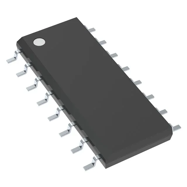
8-bit multiplying DAC in a 16-SOIC — 150 ns settling time sets the update rate
The DAC0808LCM/NOPB: The 150 ns typical settling time to ½ LSB means the output settles within one clock cycle at roughly 6.6 MSPS for a full-scale step, assuming the parallel interface can clock the data in fast enough. The multiplying architecture lets the external reference be an AC signal, so this part doubles as a digitally controlled attenuator or gain stage in a signal chain — not just a fixed DC voltage source.
Current output and external reference — the load resistor sets your voltage swing
The output is a current sink/source without an internal buffer amplifier. The designer must add an external op-amp or a load resistor to convert the current to a voltage; the output compliance range limits how high the voltage can swing before the current output saturates. The external reference means the full-scale output current is set by an external voltage and resistor — the DAC's accuracy and temperature drift follow whatever reference you choose, not an internal bandgap. The 8-bit resolution yields 256 steps; the LSB size equals the full-scale current divided by 256, so the output granularity is coarse compared to higher-resolution parts. The parallel interface ties up eight GPIOs or a parallel port — deterministic and low-latency, but pin-hungry versus a serial SPI or I²C DAC. The operating temperature range is 0°C to 75°C — commercial grade only. Not rated for industrial enclosures or automotive under-hood ambient. The 16-SOIC narrow-body footprint (1.27 mm pitch) is hand-solderable and visible-inspection friendly, so rework or prototyping is straightforward.