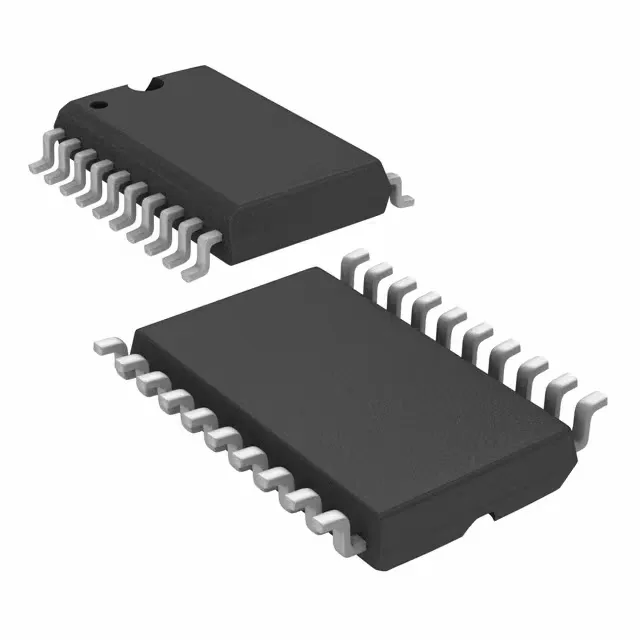
8-bit D-type with master reset
The CY74FCT273TSOC: It captures data on the positive edge of the clock and presents non-inverted outputs, with a master reset function that clears all flip-flops asynchronously. Operating from a 4.75V to 5.25V supply, this part is built for 5V logic systems. The 32mA source / 64mA sink output drive is enough to feed a bus or drive multiple CMOS inputs without external buffers.
Timing and temperature envelope
Maximum propagation delay is 13ns at 50pF load — this sets the clock-to-output timing for bus-oriented designs. At 5V, the 13ns window means the data must be stable at the input well before the next clock edge arrives, a factor when routing across a backplane or through long traces. Quiescent current is 200 µA typical, so the part adds negligible static load to the 5V rail. Input capacitance is 5 pF per pin — light enough that a single TTL or CMOS output can drive the clock line across multiple flip-flops without excessive loading.