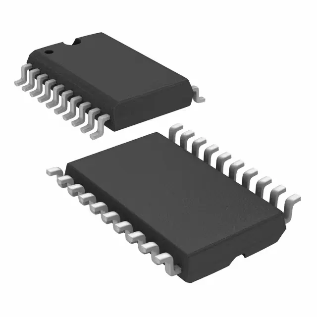
20-SOIC footprint and board integration
The CY74FCT2574ATSOC: The 5 pF input capacitance per channel means the clock line sees minimal loading; a single 33 Ω series termination resistor at the driver cleans up reflections on traces longer than 2 inches.
250 MHz clock and propagation delay budget
Positive-edge triggered D-type, eight bits per element, with a maximum clock frequency of 250 MHz. The propagation delay is 10 ns max at 5 V supply into a 50 pF load — this sets the timing margin for the data-to-clock setup window. At 250 MHz the clock period is 4 ns, so the 10 ns delay means this part is not a pipeline register at full speed; it is a bus-hold or control-register latch running at a divided clock rate, or a data-capture stage where the clock-to-Q delay is the limiting path. Output drive capability is 15 mA source, 12 mA sink — enough to drive a 50 pF load at 5 V without external buffers, but the edge rate into a higher capacitive bus will stretch the propagation delay beyond the 10 ns figure. The 200 µA quiescent current is the standby draw when the outputs are static; the dynamic current scales with the clock frequency and the number of outputs toggling.
Supply rail and temperature grade
The 10 ns propagation delay is specified at 5 V and 50 pF; derating at the low end of the supply range will add roughly 2–3 ns to the delay, so timing closure should be verified at 4.75 V and 85°C.
Active lifecycle and compliance documentation
The manufacturer provides standard compliance documentation including RoHS declaration of conformity and material composition data.