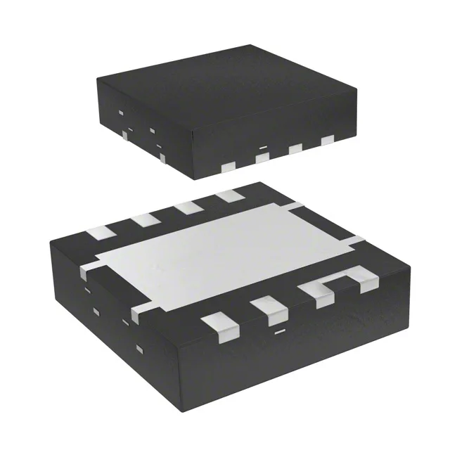
15 A in a 3.3x3.3 mm VSON — the current-density play
The CSD87333Q3DT: That current density — 15 A out of a 10.9 mm² footprint — is the headline: it lets a point-of-load converter or a battery-protection switch handle a 12 A load without moving to a larger DFN or a PowerPAK.
Conduction loss and gate-drive budget
Rds(on) is 14.3 mOhm max at 4 A with an 8 V gate drive — that is the operating point for a 12 V input POL. At 15 A the conduction loss is about 3.2 W, which sits inside the 6 W package limit but demands a solid thermal via pattern under the VSON exposed pad. The 4.6 nC gate charge at 4.5 V means a small gate-driver IC or a logic-level PWM output can switch it at several hundred kilohertz without a pre-driver stage.
ROHS3 compliant, no exemption expiry to watch.
Where it fits in the power train
Asymmetrical dual N-channel — the two FETs are not identical, which is typical for a synchronous buck where the control FET and sync FET have different Rds(on) and Qg targets. Use it in a 12 V to 1.x V POL, a battery OR-ing circuit, or a load switch where the 30 V Vdss gives headroom on a 12 V bus.