Gate charge and switching behaviour
Gate charge is 8.2 nC at 4.5 V. Input capacitance is 1250 pF at 15 V drain bias.
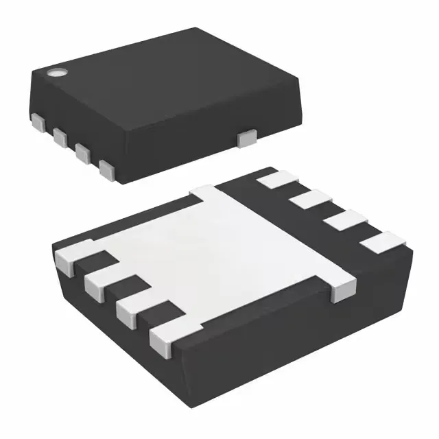
The ROHS3 compliance simplifies global BOM approvals. The 8-PowerTDFN package with exposed pad needs a solid thermal via pattern under the drain tab to keep junction temperatures within the derating curve at 27 A.
No direct pin-compatible equivalent is listed; the NexFET family includes other dual 30 V parts in different package footprints, so verify mechanical fit before substituting.