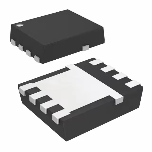
Package and thermal — the VSON-CLIP exposed pad is the thermal path
The CSD18509Q5BT comes in an 8-PowerTDFN package, also designated 8-VSON-CLIP (5x6 mm). The package is surface-mount; the clip construction reduces package resistance compared to wire-bonded alternatives of similar footprint.
Gate drive and switching — 4.5 V threshold usable, 10 V for rated Rds(on)
The drive voltage range spans 4.5 V to 10 V; the 1.2 mOhm Rds(on) is specified at 10 V, but the device can be driven from a 5 V logic rail with a higher on-resistance. The maximum gate threshold is 2.2 V at 250 µA, so a 3.3 V logic signal will not turn it on fully — a dedicated gate driver or a level-shifted PWM is needed. Input capacitance is 13900 pF at 20 V Vds; this large Ciss plus the 195 nC Qg means the driver must deliver several amperes of peak current to avoid slow switching and excessive crossover loss.
This makes the part suitable for engine bay electronics, telecom rectifiers, and outdoor power supplies where ambient temperatures can exceed 85 °C. The 150 °C TJ max provides headroom for self-heating under high-current pulsed loads.
The part is ROHS3 compliant.