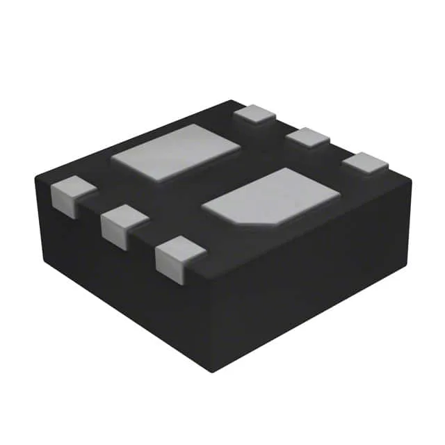
NexFET N-channel for the power loop
The CSD15571Q2 is supplied in a 6-WDFN exposed-pad package (6-SON, 2x2 mm footprint). The exposed pad conducts heat to the board copper; follow the datasheet's thermal pad layout to keep junction temperature under 150°C at full load.
Gate drive and switching speed
The gate threshold voltage maxes at 1.9 V at 250 µA drain current. Input capacitance is 419 pF at 10 V drain-source; combined with the 6.7 nC total gate charge, switching losses stay manageable into the low-MHz range for a 20 V rail. The ±20 V Vgs(max) rating gives headroom if the gate driver overshoots during hard switching — a common concern when the switching node rings on a fast turn-off.
ROHS3 compliant, no exemptions to chase for EU-market builds.