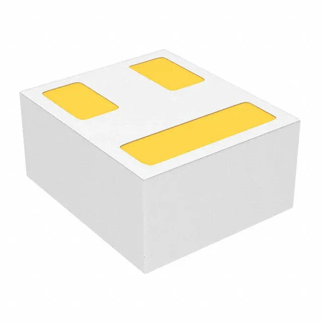
Small-signal N-channel in a 3-PICOSTAR package
It comes in a 3-XFDFN package (3-PICOSTAR supplier device package), surface-mount only. The 1190 mOhm max on-resistance at 8 V gate drive (100 mA test current) is typical for a small-signal switch — conduction loss is low enough for signal-level load switching but not for power pass-through.
Gate charge of 0.281 nC at 10 V is among the lowest in the FemtoFET™ line. Input capacitance Ciss is 10.5 pF at 10 V drain-source, so the Miller plateau is short and the turn-on/turn-off delay is dominated by the driver's source/sink resistance. The 2.8 V minimum drive voltage (for achieving the stated Rds(on)) means this MOSFET can be fully enhanced by a 3.3 V logic rail. The 8 V drive voltage gives the lowest Rds(on) — useful if the gate supply is available.
Power dissipation is 500 mW at 25 °C ambient — derate above that per the datasheet curve. The 3-PICOSTAR package has no exposed thermal pad; the die conducts heat through the solder joints and the small PCB copper area. For continuous operation near 500 mW, a two-ounce copper pour under the package is recommended.
RoHS3 compliant. No official second-source cross-reference is listed in the TI portfolio; the FemtoFET™ series is TI-specific. For dual-sourcing, a parametric search on 20 V N-channel in a 3-XFDFN with sub-1 nC gate charge would yield candidates from other vendors, but the exact footprint and electrical limits must be verified against the BOM.