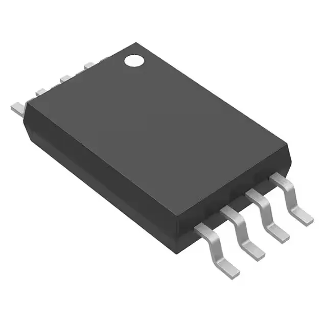
The Texas Instruments CDCVF2505PW is a single PLL clock driver in an 8-TSSOP package, designed to take one LVTTL clock input and distribute it to five LVTTL outputs with zero-delay alignment. The internal PLL locks to the input frequency and generates five synchronized copies, each capable of driving up to 200 MHz. A bypass mode lets the PLL be switched out, routing the input directly to the outputs for applications where PLL jitter or lock time is a concern. The part operates from a 3.3 V supply (3 V to 3.6 V range) and is rated for the industrial temperature span of -40°C to 85°C, making it suitable for telecom infrastructure, industrial controllers, and networking equipment where a clean, low-skew clock tree is needed across multiple loads.
The 200 MHz maximum frequency sets the upper bound for the input clock and output switching. The 1:5 fanout ratio means one input drives five outputs.
PLL with bypass — when to use each mode
The PLL mode provides zero-delay clock alignment, meaning the output edges are phase-aligned to the input edge, which is critical for synchronous designs where clock skew between loads must be minimized. Bypass mode disables the PLL and routes the input directly to the outputs — use this when the input clock is already clean and jitter-free, or when the PLL's lock transient at power-up could cause timing violations in the downstream logic. The bypass feature is a practical differentiator: it lets the same board design handle both PLL-synchronized and direct-through clock trees without a separate part.
Package and mounting — 8-TSSOP surface mount
Surface-mount assembly is standard.
The ROHS3 status means it meets the latest EU restriction levels for lead and other hazardous substances — no exemption expiry to track.