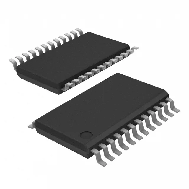
Texas Instruments CDCVF2310PW — Clock & Timing ICs

CDCVF2310PW Texas Instruments 1:10 LVTTL Fanout Buffer 200

MPNCDCVF2310PW
End of Life

Texas Instruments CDCVF2310PW, Fanout Buffer (Distribution), 1:10 LVTTL, 200 MHz max, 2.3V–3.6V supply, 24-TSSOP, -40°C to 85°C.

$6.92Ref. price · indicative, final on quote
Packaging24-TSSOP (0.173", 4.40mm Width)
StockContact for availability
MOQ1 pcs
  • 100% new & originalTraceable channels only — no refurbs, no pulls, no remarked parts.
  • Date & lot codes on quoteStated per line before you commit; label photos on request.
  • MSL-compliant ESD packingMoisture-sealed bags with indicator cards; reels photo-verified.
  • PayPal buyer protectionPay by T/T, PayPal or Payoneer — card payments covered end to end.

Specifications

CDCVF2310PW Technical Specifications
ParameterValue
TypeFanout Buffer (Distribution)
Mounting typeSurface Mount
Voltage2.3V ~ 3.6V
Frequency200 MHz
Operating temperature-40°C ~ 85°C
InputLVTTL
OutputLVTTL
PackageTube
Case24-TSSOP (0.173\", 4.40mm Width)
Number of circuits1
Ratio - Input:Output1:10
Differential - Input:OutputNo/No

Product details

1:10 LVTTL clock distribution at 200 MHz

The CDCVF2310PW is a 1:10 fanout buffer from Texas Instruments, accepting a single LVTTL input and delivering ten LVTTL outputs at up to 200 MHz. This part is designed for clock distribution in systems where a single clock source must drive multiple loads without degrading signal integrity. The non-differential I/O (LVTTL in/out) keeps the BOM simple and the layout straightforward — no external termination resistors needed for differential pairs.

Fanout ratio and supply flexibility

With a 1:10 fanout ratio, a single LVTTL clock source can feed ten downstream devices — enough for a moderate clock tree without needing a second buffer stage. The wide supply range (2.3V–3.6V) means the same part can be used across 2.5V and 3.3V domains, reducing inventory complexity.

Active production and compliance

It is ROHS3 compliant, so it meets current European and global environmental requirements for lead-free assembly. The part is supplied in a tube (24-TSSOP package). Confirm the BOM's preferred packaging before ordering.

Package and layout considerations

The 24-TSSOP package (0.173-inch body width, 4.40 mm) is a fine-pitch SMD package that requires careful PCB layout. Supply decoupling is critical for clock buffers: place a 0.1 µF ceramic capacitor as close as possible to each supply pin, with a bulk capacitor (10 µF) nearby. The wide supply range (2.3V–3.6V) gives some margin for rail noise, but the output jitter will degrade if the supply is noisy.

Frequently asked questions

What is the difference between CDCVF2310PW and CDCVF2310PWR?

The electrical specifications are identical. The PW suffix indicates tube packaging; the PWR suffix indicates tape-and-reel packaging. Choose based on your assembly line's feeder requirements.

What is the maximum frequency of CDCVF2310PW?

The maximum frequency is 200 MHz, specified for LVTTL input and output. This is the ceiling for the clock signal the buffer can distribute cleanly.