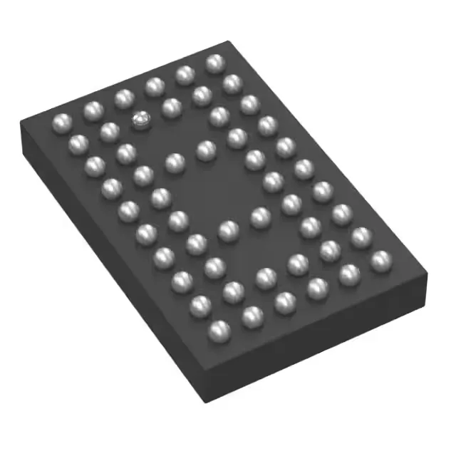
Texas Instruments CDCU2A877NMKT — Discrete Semiconductors

TI CDCU2A877NMKT PLL Clock Driver, 410 MHz, 1:10, DDR2

MPNCDCU2A877NMKT
End of Life

Texas Instruments CDCU2A877NMKT, 1.8V phase-lock loop clock driver, PLL Yes, Input Clock, Output Clock, 1:10 ratio, 410 MHz max, differential I/O, 52-NFBGA (7x4.5 mm), ROHS3 compliant.

$10.31Ref. price · indicative, final on quote
Packaging52-VFBGA
RoHSROHS3 Compliant
Independent supplier — new & surplus stockAuthenticity-screened · ESD-safe packingListing updated Aug 2026

Specifications

CDCU2A877NMKT specifications
ParameterValue
MountingSurface Mount
Supply voltage1.7V ~ 1.9V
Frequency - max410MHz
Operating temperature0°C ~ 70°C (TA)
PLLYes
InputClock
OutputClock
PackageTape & Reel (TR); Cut Tape (CT)
Main purposeMemory, DDR2
Case52-VFBGA
Number of circuits1
Ratio - Input:Output1:10
Differential - Input:OutputYes/Yes

Product details

DDR2 clock distribution with integrated PLL

The Texas Instruments CDCU2A877NMKT is a 1.8V phase-lock loop clock driver designed specifically for DDR2 memory systems. It takes one clock input and fans it out to ten differential clock outputs (1:10 ratio), providing the low-jitter, matched-delay clock trees that DDR2 DIMMs require for reliable read/write timing. With a maximum frequency of 410 MHz, this part comfortably covers DDR2-800 and slower memory interfaces. The differential input and output (Yes/Yes per the spec) keep common-mode noise rejection high, which matters when routing clocks across a multi-layer motherboard.

No additional regulator is needed if the memory bus is already at 1.8V. This suits desktop, server, and networking equipment in climate-controlled environments but is not rated for extended industrial or automotive ambient ranges.

The CDCU2A877NMKT comes in a 52-VFBGA package (supplier device package 52-NFBGA, 7x4.5 mm). This is a fine-pitch BGA — hand-soldering is impractical; a controlled SMT reflow profile with stencil-printed solder paste is the standard assembly method. Surface-mount mounting type and the small footprint make it suitable for dense PCB layouts where clock distribution must sit close to the memory controller or DIMM slots to minimise trace skew.

ROHS3 compliant — no exemptions that might complicate EU or other regulated-market shipments. No additional compliance documentation (REACH, UL, IEC) is cited in the available record.

Frequently asked questions

What is the 1:10 ratio used for in a DDR2 system?

The 1:10 fanout (one input, ten differential outputs) lets a single PLL clock driver feed multiple DDR2 DIMMs or a memory controller plus several DIMMs from one low-jitter source, keeping skew between clock lanes within the DDR2 timing budget.

What supply voltage does CDCU2A877NMKT need?

It operates from 1.7V to 1.9V, which matches the standard DDR2 VDDQ rail of 1.8V ±0.1V. No extra voltage regulator is required if the memory bus is already at 1.8V.

Can I hand-solder the 52-NFBGA package?

The 52-VFBGA (7x4.5 mm) is a fine-pitch BGA — hand-soldering is not practical. A controlled SMT reflow profile with stencil-printed solder paste is the standard assembly method.