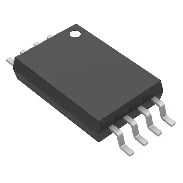
Texas Instruments CDCS504TPWRQ1 — Clock & Timing ICs

CDCS504TPWRQ1 Clock Multiplier, 108 MHz, 8-TSSOP, AEC-Q100

MPNCDCS504TPWRQ1
End of Life

Texas Instruments CDCS504TPWRQ1 clock multiplier, 108 MHz max, LVCMOS input/output, 3V to 3.6V supply, single circuit, 1:1 ratio, 8-TSSOP package, AEC-Q100 automotive qualified.

$1.65Ref. price · indicative, final on quote
Packaging8-TSSOP (0.173", 4.40mm Width)
RoHSROHS3 Compliant
SeriesAutomotive, AEC-Q100
Independent supplier — new & surplus stockAuthenticity-screened · ESD-safe packingListing updated Aug 2026

Specifications

CDCS504TPWRQ1 specifications
ParameterValue
TypeMultiplier
SeriesAutomotive, AEC-Q100
MountingSurface Mount
Voltage3V ~ 3.6V
Frequency108 MHz
Operating temperature-40°C ~ 105°C
InputLVCMOS
OutputLVCMOS
PackageTape & Reel (TR); Cut Tape (CT)
Case8-TSSOP (0.173\", 4.40mm Width)
Number of circuits1
Ratio - Input:Output1:1
Differential - Input:OutputNo/No

Product details

What the 108 MHz ceiling means for your clock tree

The CDCS504TPWRQ1 is a single-channel LVCMOS clock multiplier in an 8-TSSOP package, rated for a maximum output frequency of 108 MHz. That 108 MHz is the hard ceiling — the multiplied clock cannot exceed it, so the input frequency times the internal multiplication factor must land at or below that value. The input and output are both LVCMOS — single-ended, standard CMOS levels. No differential termination, no CML or LVPECL translation resistors. The single-circuit topology keeps the package small and the routing direct, but it also means the multiplied clock serves exactly one load.

Automotive temperature grade and the board environment

The 105°C upper limit places it in the cabin or under-hood zone where the electronics see conducted heat from the engine bay but not direct exhaust-manifold temperatures. For a timing tree in an automotive ECU, this temperature grade means the multiplier's output jitter and frequency accuracy are characterized across the full range, not just at 25°C.

Frequently asked questions

What is the maximum output frequency of CDCS504TPWRQ1?

The maximum output frequency is 108 MHz. The input frequency multiplied by the internal multiplication factor must not exceed this ceiling. The input and output are both LVCMOS, single-ended, with a 1:1 input-to-output ratio.

What compliance documentation does Texas Instruments provide for CDCS504TPWRQ1?

Texas Instruments provides ROHS3 compliance certification and AEC-Q100 automotive qualification documentation for the CDCS504TPWRQ1.