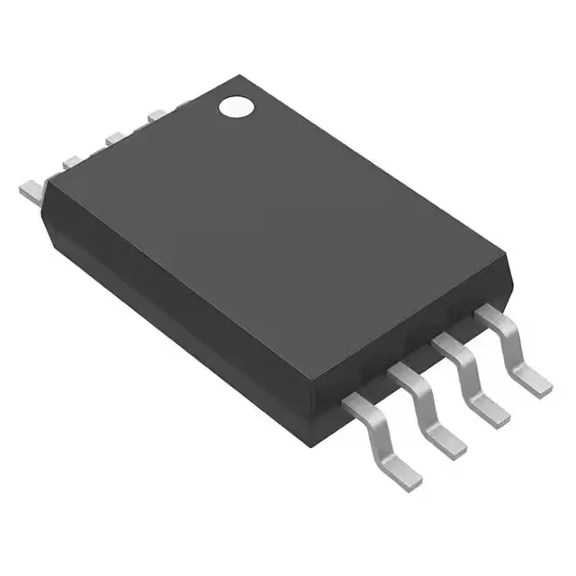
Single-supply LVCMOS clock buffer, 108 MHz ceiling
The CDCS503PW is a 1:1 clock buffer and multiplier accepting LVCMOS input and delivering LVCMOS output, with a maximum operating frequency of 108 MHz. The 108 MHz ceiling sets the practical limit for the downstream clock domain — any load capacitance or trace length that adds jitter beyond this frequency will push the output edge rate past the buffer's drive capability. For a 3.3V LVCMOS clock tree feeding FPGAs, ASICs, or SERDES reference clocks, this buffer is suited to frequencies up to that maximum.
Industrial temperature grade, 8-TSSOP footprint
No exposed thermal pad — junction-to-ambient thermal resistance is managed by the copper trace area on the PCB, which for a 3.3V buffer drawing a few mA is rarely a constraint.