What the 1:12 fanout buys you on a clock tree
The CDCLVC1112PWR takes one LVCMOS clock input and distributes it to twelve outputs with a 250 MHz ceiling — enough to feed a dozen synchronous loads from a single oscillator without adding separate buffer stages. The 1:12 ratio means this single 24-TSSOP part replaces a cascade of smaller fanout buffers, saving board area and reducing the total propagation delay through the clock tree. Input and output levels are both LVCMOS and the path is non-differential (No/No per the datasheet), so this part fits designs where the reference clock is a single-ended CMOS oscillator or a crystal-driven PLL output — common in FPGA reference clock distribution, baseband processor clock trees, and Ethernet switch timing.
Supply voltage and temperature range — what they mean for the BOM
No external regulator is needed when the buffer shares the same rail as the FPGA bank it feeds, which keeps the BOM count low. For outdoor telecom or industrial control enclosures that see -20°C startup, the propagation delay and output skew stay within the datasheet limits without derating.
Package and board-fit for the layout engineer
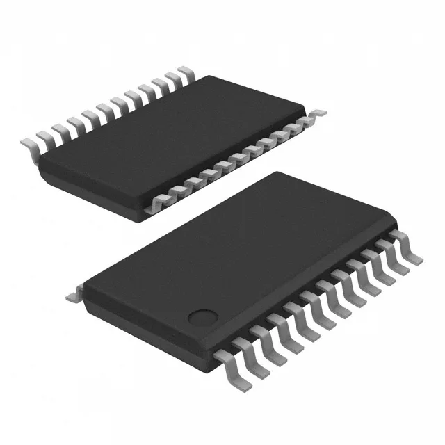
The 24-TSSOP body (4.40 mm wide, 0.65 mm pin pitch) is a standard footprint that routes easily on two-layer boards — the outer pins carry the supply and ground, the inner pins are the clock outputs. The 0.173-inch (4.40 mm) width keeps the package narrow enough to fit between dense BGA keep-out zones on a multi-layer backplane. The supplier device package (24-TSSOP) matches the package/case entry — no footprint variation between the two fields.
Lifecycle and compliance — what the procurement desk needs
ROHS3 compliant per the manufacturer's declaration.