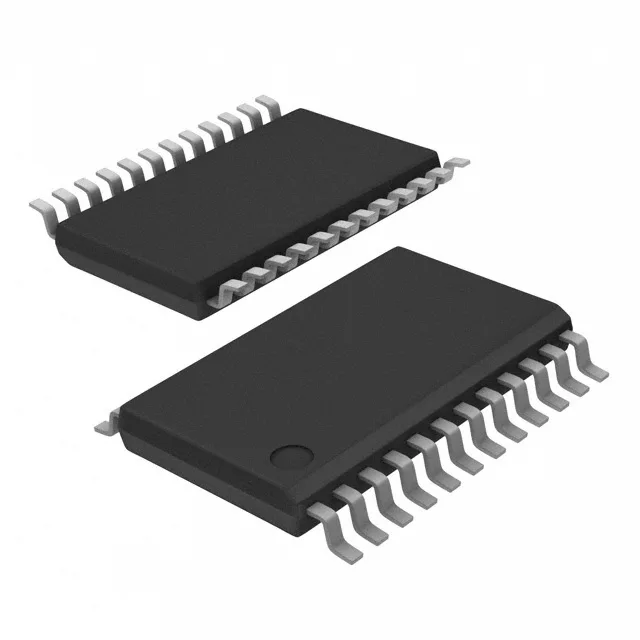
1:12 LVCMOS fanout buffer for single-ended clock trees
The Texas Instruments CDCLVC1112PW is a 1:12 fanout buffer designed for distributing single-ended LVCMOS clock signals across a PCB. It accepts one LVCMOS input and delivers twelve identical LVCMOS outputs, each capable of driving up to 250 MHz. The wide supply range of 2.3 V to 3.6 V lets it operate from either a 2.5 V or 3.3 V rail without an intermediate regulator, simplifying the power architecture.
The 250 MHz maximum frequency sets the upper bound for the input clock this buffer can pass without introducing excessive edge-rate degradation or additive jitter. For a system clock running at 200 MHz, the part has 50 MHz of headroom, which keeps propagation delay and output-to-output skew within the datasheet limits. If your design uses a faster serial interface clock (e.g., 312.5 MHz for a 10G Ethernet reference), this part will not cleanly pass it — you would need a higher-speed fanout buffer. The 1:12 ratio means a single input can feed twelve loads, which is useful for distributing a reference clock to multiple FPGAs, ADCs, or PHYs on a dense board.
Non-differential I/O — single-ended only
Both the input and output are specified as LVCMOS, and the differential flag is No/No. This part cannot buffer LVPECL, LVDS, or CML signals directly. If your clock source is differential, you will need a converter (e.g., a resistor network or a dedicated translator) before feeding this buffer. The non-differential nature also means the outputs are single-ended, so trace-length matching and impedance control matter more for signal integrity at higher frequencies.
This makes the part safe to qualify into a production BOM for a multi-year program without worrying about an imminent discontinuation. The 24-TSSOP package is a standard, widely second-sourced footprint, so alternative distributors can supply it if the primary channel tightens.
24-TSSOP — board area and routing considerations
The 24-TSSOP package (0.173" body width, 4.40 mm) is a fine-pitch surface-mount package that saves board space compared to a wider SOIC. With twelve outputs, the pinout is dense — expect to route the output traces with matched lengths if the clock is timing-critical.