230 MHz spread-spectrum clock fan-out for automotive noise budgets
The CDCE949QPWRQ1 is a Texas Instruments automotive-grade spread spectrum clock driver with an integrated PLL that includes a bypass mode. It accepts either an LVCMOS reference or a crystal input and distributes a single clean clock to nine LVCMOS outputs, each capable of running up to 230 MHz. Spread spectrum modulation spreads the output energy across a wider frequency band, reducing peak EMI radiated from the clock traces and the attached digital loads. For an automotive ECU or infotainment head unit that must pass CISPR 25, this part shifts the compliance margin without adding ferrite beads or shielding cans.
PLL bypass mode — when the reference is clean enough
The PLL can be bypassed entirely, routing the input clock straight to the output buffers. This is useful when the incoming reference is already frequency-locked and jitter-controlled — for example, a master clock from an FPGA or a TCXO — and you want zero added phase noise from the PLL loop filter. When the PLL is active, the internal divider/multiplier allows synthesising a different output frequency from the input reference. The 1:9 fan-out ratio means a single crystal or oscillator can feed nine downstream loads — ADCs, SoCs, SerDes reference inputs — without external clock buffers.
If your board already has a 1.8 V rail, this part drops straight onto it without an extra regulator. The narrow tolerance means the rail must stay within 1.7 V–1.9 V under load transients — a 1.8 V LDO with ±3 % regulation is adequate.
Qualified to AEC-Q100, the CDCE949QPWRQ1 is rated for automotive stress conditions including high-temperature operating life and moisture sensitivity.
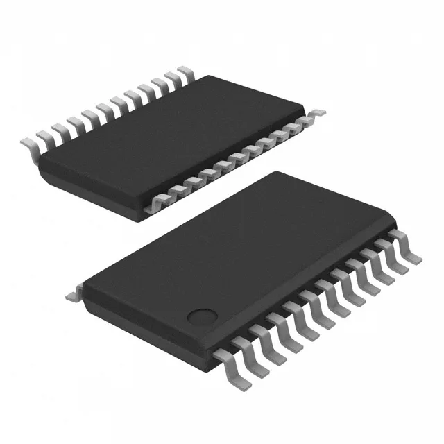
24-TSSOP footprint — layout checklist
The 0.65 mm pitch allows two-layer breakout with 0.25 mm traces and 0.30 mm vias, though a four-layer stack is recommended for the 1.8 V rail and the nine output traces to keep impedance controlled.