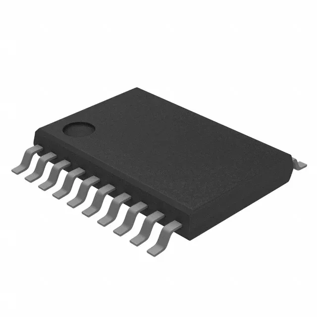
Texas Instruments CDCE937QPWRQ1 — Clock & Timing ICs

CDCE937QPWRQ1 Clock Driver, 230 MHz, AEC-Q100, TSSOP-20

MPNCDCE937QPWRQ1
Active

Texas Instruments CDCE937QPWRQ1 Automotive Spread Spectrum Clock Driver, PLL with Bypass, LVCMOS Input/Output, 230 MHz Max, 1:7 Fanout, 20-TSSOP Package.

$3.3330Ref. price · indicative, final on quote
Independent supplier — new & surplus stockAuthenticity-screened · ESD-safe packingListing updated Aug 2026

Specifications

CDCE937QPWRQ1 specifications
ParameterValue
TypeSpread Spectrum Clock Driver
SeriesAutomotive, AEC-Q100
MountingSurface Mount
Supply voltage1.7V ~ 1.9V
Frequency - max230MHz
Operating temperature-40°C~125°C
PLLYes with Bypass
InputLVCMOS, Crystal
OutputLVCMOS
PackageTape & Reel (TR); Cut Tape (CT)
Case20-TSSOP (0.173\", 4.40mm Width)
Divider (Multiplier)Yes/No
Number of circuits1
Ratio - Input:Output1:7
Differential - Input:OutputNo/No

Product details

Active production — AEC-Q100 spread-spectrum clock fanout

The CDCE937QPWRQ1: It integrates a PLL with bypass mode and delivers a 1:7 LVCMOS fanout from either a crystal or LVCMOS reference, with a maximum output frequency of 230 MHz — enough to clock the main bus, memory interface, and peripheral domains from a single device. The spread-spectrum modulation spreads the clock energy across a wider frequency band, reducing peak EMI at the fundamental and its harmonics by several dB — a practical advantage when the PCB layout has to pass CISPR 25 radiated emissions without a metal shield can.

1.7 V to 1.9 V supply, 20-TSSOP package

Operating from a single 1.7 V to 1.9 V rail, the CDCE937QPWRQ1 sits on the low-voltage core supply common in automotive infotainment and ADAS processors — no separate 3.3 V clock rail is needed. All seven LVCMOS outputs are non-differential, and the part does not include a divider on the output side — the 1:7 fanout is a straight buffer with spread-spectrum modulation applied to the output clock tree.

Frequently asked questions

What is the input and output signal type for CDCE937QPWRQ1?

The input accepts either an LVCMOS reference or a crystal; all seven outputs are LVCMOS. There are no differential I/O paths on this device.