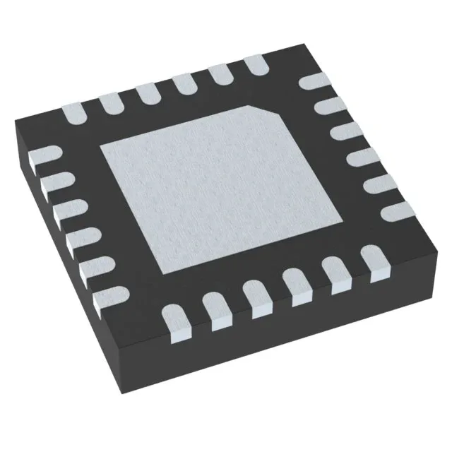
Texas Instruments CDCE6214TWRGETQ1 — Clock & Timing ICs

CDCE6214TWRGETQ1 Clock Generator, 350 MHz, AEC-Q100, QFN-24

MPNCDCE6214TWRGETQ1
Active

Texas Instruments CDCE6214TWRGETQ1, Automotive AEC-Q100 Clock Generator, PLL Yes, 350 MHz max, HCSL/LVCMOS/LVDS output, 1.71V–3.465V supply, -40°C to 105°C, 24-VQFN Exposed Pad.

$7.3100Ref. price · indicative, final on quote
Independent supplier — new & surplus stockAuthenticity-screened · ESD-safe packingListing updated Aug 2026

Specifications

CDCE6214TWRGETQ1 specifications
ParameterValue
TypeClock Generator
SeriesAutomotive, AEC-Q100
MountingSurface Mount, Wettable Flank
Voltage1.71V ~ 3.465V
Frequency350MHz
Operating temperature-40°C~105°C(TA)
PLLYes
InputDifferential or Single-Ended
OutputHCSL, LVCMOS, LVDS
PackageTape & Reel (TR); Cut Tape (CT)
Case24-VFQFN Exposed Pad
Divider (Multiplier)Yes/No
Number of circuits1

Product details

350 MHz PLL clock generator for automotive SERDES and ADAS timing

It integrates a PLL and supports differential or single-ended inputs, producing output clocks in HCSL, LVCMOS, or LVDS formats at up to 350 MHz.

Output flexibility eliminates level translators

Three output standards — HCSL for PCIe reference clocks, LVDS for long-reach differential distribution, and LVCMOS for single-ended fan-out — let the same part drive multiple clock domains without external translation. The 350 MHz ceiling supports the SERDES reference clocks in ADAS camera links and infotainment video buses.

Package and mounting — QFN with wettable flank

Housed in a 24-VFQFN with exposed pad (4x4 mm body), the wettable flank option improves solder-joint inspection yield for automated optical inspection (AOI) in high-volume automotive assembly. Surface-mount with wettable flank is the preferred footprint for under-hood modules that undergo thermal cycling.

RoHS compliance is standard for the series.

Frequently asked questions

What output formats does the CDCE6214TWRGETQ1 support?

The device outputs HCSL, LVCMOS, and LVDS clock signals, selectable per the configuration. This range covers PCIe reference clocks (HCSL), long-reach differential distribution (LVDS), and single-ended fan-out (LVCMOS) without external level translation.