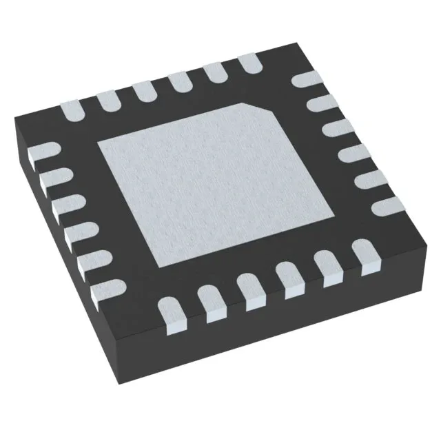
Texas Instruments CDCE6214TWRGERQ1 — Clock & Timing ICs

TI CDCE6214TWRGERQ1 Clock Generator, 350 MHz, AEC-Q100

MPNCDCE6214TWRGERQ1
Active

Texas Instruments CDCE6214TWRGERQ1 automotive clock generator, integrated PLL, 350 MHz max frequency, HCSL/LVCMOS/LVDS outputs, 1.71 V to 3.465 V supply, 24-VQFN with wettable flank, AEC-Q100 Grade 1.

$6.9600Ref. price · indicative, final on quote
Independent supplier — new & surplus stockAuthenticity-screened · ESD-safe packingListing updated Aug 2026

Specifications

CDCE6214TWRGERQ1 specifications
ParameterValue
TypeClock Generator
SeriesAutomotive, AEC-Q100
MountingSurface Mount, Wettable Flank
Supply voltage1.71V ~ 3.465V
Frequency - max350MHz
Operating temperature-40°C~105°C(TA)
PLLYes
InputDifferential or Single-Ended
OutputHCSL, LVCMOS, LVDS
PackageTape & Reel (TR); Cut Tape (CT)
Case24-VFQFN Exposed Pad
Divider (Multiplier)Yes/No
Number of circuits1

Product details

350 MHz PLL clock generator for automotive timing trees

The CDCE6214TWRGERQ1 is a single-circuit PLL-based clock generator from Texas Instruments, qualified to AEC-Q100 for automotive applications. Its 350 MHz maximum output frequency suits reference clock generation for SerDes, high-speed ADCs, or PCIe interfaces in infotainment and ADAS domains.

Supply flexibility and output types

Output options include HCSL, LVCMOS, and LVDS, matching PCIe reference clocks, general-purpose logic distribution, or differential clock lines. The input accepts differential or single-ended references, and the integrated divider/multiplier allows frequency synthesis without an external VCXO. The single PLL circuit targets point-of-use clock cleaning or frequency translation in a compact footprint.

Frequently asked questions

What output types does the CDCE6214TWRGERQ1 support?

The device outputs HCSL, LVCMOS, and LVDS. HCSL is typical for PCIe reference clocks, LVDS for differential distribution, and LVCMOS for single-ended logic-level clocking.