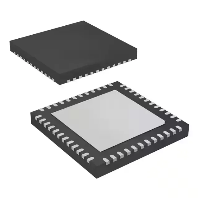
The CDCE62005RGZT is a TI clock generator with an integrated PLL that supports a bypass mode, allowing the VCO to be disabled and the reference clock to pass through directly — useful for system test or when a clean external clock source is available. The maximum output frequency of 1.5 GHz makes this part suitable for clocking high-speed SerDes transceivers, FPGA transceiver banks, and RF sampling converters where jitter performance at multi-GHz frequencies is critical. Input and output ports accept LVCMOS, LVDS, and LVPECL standards, plus a crystal input on the reference side, so it can bridge between legacy 3.3 V CMOS clock trees and differential CML/LVPECL fan-out networks without external level translators.
3:5 fan-out and differential signalling — BOM-fit detail
The 3-to-5 input-to-output ratio lets the device accept up to three reference clocks and distribute five cleaned copies — enough to feed five separate SerDes devices or FPGA banks from a single PLL clean-up stage. Both the input and output paths support differential signalling, so the part can accept a differential reference (e.g. LVDS from an OCXO) and deliver LVPECL fan-out to downstream receivers without single-ended-to-differential conversion.
Lifecycle status is Active, meaning TI continues to manufacture this part with no announced last-time-buy or discontinuation. No successor has been issued — the CDCE62005RGZT is the current production variant of the base CDCE62005 clock generator family.