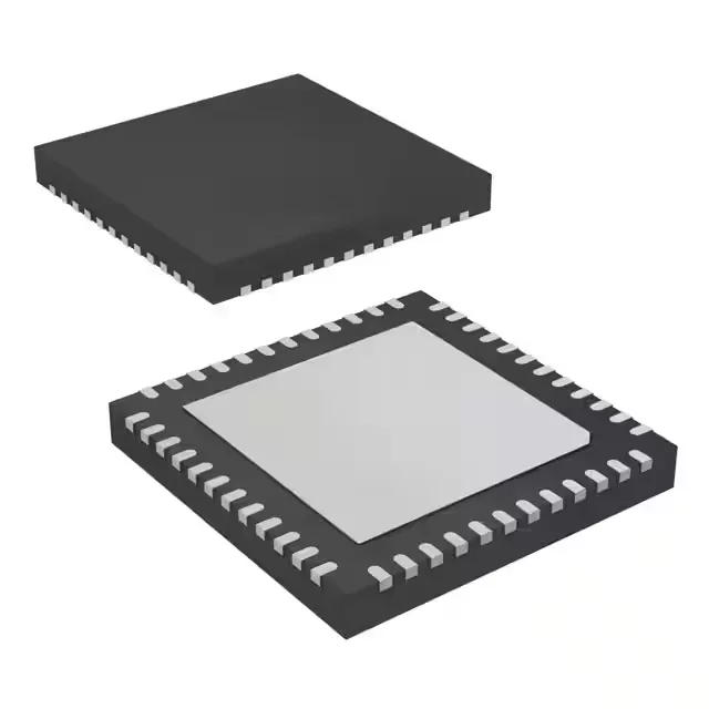
CDCE62005RGZR

Texas Instruments

Texas Instruments CDCE62005RGZR Clock Generator, PLL with Bypass, 1.5 GHz max, 3:5 Input:Output, LVCMOS/LVDS/LVPECL/Crystal I/O, 48-VFQFN Exposed Pad, -40°C to 85°C.

Texas Instruments CDCE62005RGZR
Download datasheet (PDF)
[IN STOCK] In Stock: 9 pcs
$17.23/ pc

Volume pricing

Buy Now

MOQ 1 · Tape & Reel (TR); Cut Tape (CT) · RoHS · EIA-481 · DAP/DDP · T/T

Technical specifications

CDCE62005RGZR specifications
Parameter / AttributeSpecification / Value
TypeClock Generator
MountingSurface Mount
Supply voltage3V ~ 3.6V
Frequency - max1.5GHz
Operating temperature-40°C~85°C
PLLYes with Bypass
InputLVCMOS, LVDS, LVPECL, Crystal
OutputLVCMOS, LVDS, LVPECL
PackageTape & Reel (TR); Cut Tape (CT)
Case48-VFQFN Exposed Pad
Divider (Multiplier)Yes/No
Number of circuits1
Ratio - Input:Output3:5
Differential - Input:OutputYes/Yes

Technical details

1.5 GHz clock synthesis with multi-protocol I/O

The CDCE62005RGZR is a clock generator from Texas Instruments integrating a PLL with bypass mode, capable of synthesizing output clocks up to 1.5 GHz from a single reference input. It accepts LVCMOS, LVDS, LVPECL, or crystal inputs and can deliver the same output formats, making it suitable for clock trees that must bridge different logic families on the same board. The 3:5 input-to-output ratio allows up to five independent clock domains from one reference, reducing the number of oscillators in a design.

Housed in a 48-VFQFN with exposed pad (7x7 mm), the package requires a thermal land on the PCB for heat sinking — the exposed pad must be soldered to the ground plane to achieve the rated thermal performance. Surface-mount assembly; the 0.5 mm pitch QFN demands careful stencil design and reflow profile control to avoid solder bridging.

CDCE62005RGZR
[ALLOC] verified
Quote