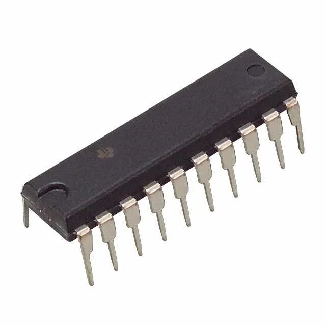
The CD74HCT377E is supplied in a 20-pin PDIP (0.300-inch body, 7.62 mm width) through-hole package. The 0.100-inch row spacing and 0.100-inch pin pitch match standard breadboard and prototyping grids, but the 0.300-inch body width requires a DIP-20 socket or plated through-hole pattern with 0.300-inch row centers — not the narrower 0.200-inch footprint used by some 20-pin SOIC or SSOP parts. The 10 pF input capacitance per pin is typical for HCT logic; no special decoupling beyond a 0.1 µF ceramic per supply pin is required for the 50 MHz clock rate.
Timing and drive for 5 V backplanes
With a maximum clock frequency of 50 MHz and a propagation delay of 38 ns at 4.5 V with a 50 pF load, this flip-flop is sized for bus-register and address-latch applications in 5 V TTL systems. The 38 ns delay includes the output rise time into the load; at 50 MHz the period is 20 ns, so the device cannot toggle at full clock rate with the output driving a heavy bus — the delay limits the usable data rate to roughly 26 MHz when driving a 50 pF trace. The 4 mA source and 4 mA sink output drive provides a fan-out of 10 LSTTL loads (each drawing 0.4 mA) with adequate noise margin. For longer backplane traces or higher capacitive loads, a bus driver or buffer should be inserted between the flip-flop output and the bus.
The 125°C upper limit is the junction temperature; the PDIP package's thermal resistance (typically 60-80°C/W in still air) means the device can dissipate about 0.5 W before exceeding the 125°C limit at 25°C ambient.
ROHS3 compliance means no exemptions for lead in solder or other restricted substances — the part can be used in EU, UK, and global BOMs without exemption tracking.