74HCT quad D-type with master reset — what the ratings mean for the BOM
The CD74HCT175E is a quad D-type flip-flop from the 74HCT series, packing four positive-edge-triggered flip-flops with complementary outputs and a common master reset into a 16-pin DIP. Each of the four bits latches the D input on the rising clock edge; the complementary Q and Q̅ outputs drive up to 4 mA source or sink, enough to directly feed a downstream logic gate or a low-current LED indicator without a buffer. The 25 MHz clock frequency and 33 ns max propagation delay at 4.5 V into 50 pF set the timing budget: the part reliably captures data at clock rates up to 25 MHz, but the propagation delay means the Q output settles 33 ns after the clock edge — the downstream logic must wait that long before sampling. For a 25 MHz clock (40 ns period), the 33 ns delay consumes 82% of the cycle, leaving only 7 ns of setup margin at the next stage; designs running near the ceiling should account for this. Operating temperature spans -55°C to +125°C, which covers military and industrial thermal environments — the part is not AEC-Q qualified, but the temperature range suits avionics bays, engine compartments with active cooling, or outdoor telecom cabinets where commercial-grade parts would derate. Supply voltage is 4.5 V to 5.5 V, so it runs from a standard 5 V rail with ±10% tolerance; the 74HCT family is TTL-compatible on the input thresholds, meaning a 5 V TTL output drives it directly without a level shifter.
Package, footprint, and integration
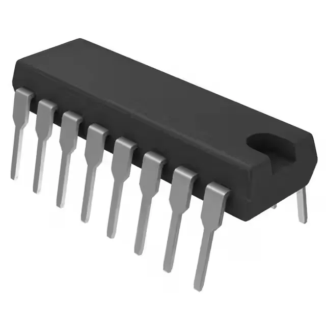
Housed in a 16-DIP with 0.300-inch row spacing and 7.62 mm body width, the CD74HCT175E is a through-hole part that drops into a standard DIP-16 socket or solders directly into plated through-holes on a 0.100-inch pitch grid. The supplier device package is 16-PDIP — the plastic dual-in-line variant. No exposed pad, no thermal vias needed; the 8 µA quiescent current means self-heating is negligible, so no thermal derating beyond the datasheet's ambient limits. Input capacitance is 10 pF per pin — the clock line sees this load, so at 25 MHz the dynamic power draw is modest but the clock driver must still source the charge per edge. The master reset input is asynchronous: when pulled low, all Q outputs go low and Q̅ outputs go high regardless of the clock state. Unused inputs should be tied to VCC or GND to prevent floating-node oscillation; the complementary outputs can be left open if only one polarity is needed.