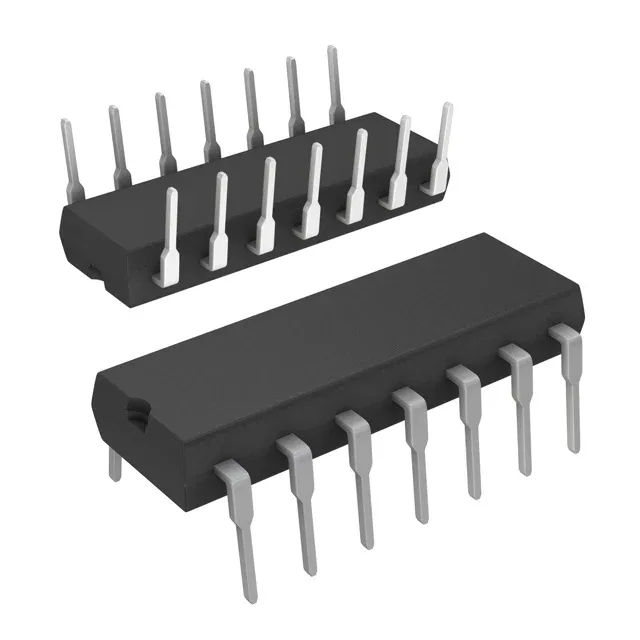
Texas Instruments CD74HCT107E — Discrete Semiconductors

Texas Instruments CD74HCT107E JK Flip-Flop, 56 MHz, 14-DIP

MPNCD74HCT107E
End of Life

Texas Instruments 74HCT series JK Type flip-flop, CD74HCT107E, dual 1-bit, negative-edge triggered, complementary output, 56 MHz, 14-DIP, through hole, -55 to 125°C.

$1.19Ref. price · indicative, final on quote
Packaging14-DIP (0.300", 7.62mm)
RoHSROHS3 Compliant
Series74HCT
Independent supplier — new & surplus stockAuthenticity-screened · ESD-safe packingListing updated Aug 2026

Specifications

CD74HCT107E specifications
ParameterValue
TypeJK Type
Series74HCT
Output typeComplementary
Trigger typeNegative Edge
MountingThrough Hole
Supply voltage4.5V ~ 5.5V
Current - quiescent4 µA
Current - output high, low4mA, 4mA
Clock frequency56 MHz
Operating temperature-55°C ~ 125°C (TA)
PackageTube
FunctionReset
Case14-DIP (0.300\", 7.62mm)
Input capacitance10 pF
Number of elements2
Number of bits per element1
Max propagation delay @ v, max CL43ns @ 4.5V, 50pF

Product details

Dual JK flip-flop in a 14-pin DIP

The CD74HCT107E: Each of the two elements stores one bit and toggles on the negative edge of the clock input, with a complementary output pair per flip-flop. The reset function overrides the clock and sets the outputs to a known state. Rated for a clock frequency up to 56 MHz, the part suits moderate-speed logic chains in through-hole designs where a 5 V rail is already present.

Temperature grade and output drive

This makes it viable for avionics bay, engine test cell, or outdoor telecom enclosures where the ambient swings well beyond commercial 0-70°C limits. Each output sinks or sources 4 mA (at Vcc = 4.5 V), which is typical for HCT family gates. The 4 mA drive directly interfaces with standard CMOS inputs and most TTL loads without a buffer stage. Propagation delay is 43 ns maximum at 4.5 V with a 50 pF load — this sets the timing budget for cascaded stages: two flip-flops in series add 86 ns of clock-to-output latency before the next logic decision. Quiescent current is 4 µA typical, so the part adds negligible static draw to the supply rail. Input capacitance is 10 pF per input, which matters for clock line loading when multiple flip-flops share a common clock trace.

Package and board-fit

Housed in a 14-pin PDIP (0.300-inch, 7.62 mm body width), the CD74HCT107E is a through-hole part that mounts directly into a standard 0.100-inch pitch DIP socket or solders into plated through-holes on a 2.54 mm grid. The 14-PDIP footprint is one of the most widely supported IC packages — it fits perfboard, stripboard, and most prototype PCBs without a custom footprint.

Frequently asked questions

What is the CD74HCT107E's clock frequency and propagation delay?

The CD74HCT107E is rated for a maximum clock frequency of 56 MHz. Its maximum propagation delay is 43 ns at 4.5 V supply with a 50 pF load. This means the flip-flop's output settles within 43 ns after the clock edge, which sets the timing margin for downstream logic.

Does the CD74HCT107E have a reset function?

Yes, the CD74HCT107E includes a reset input per flip-flop. When the reset pin is asserted, the flip-flop output is forced to a known state regardless of the clock or J/K inputs. This is useful for initializing counters or state machines to a known condition on power-up.