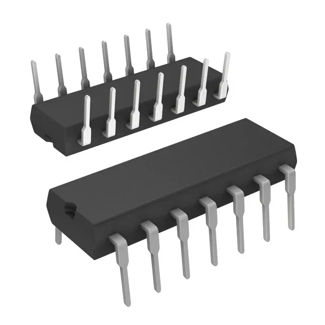
Package and integration story
The CD74HC73E comes in a 14-pin DIP (0.300-inch body) with a through-hole PDIP footprint — the same 0.100-inch pitch layout that has been a breadboard and perfboard staple for decades. The 7.62 mm row spacing means it drops into standard socket strips or wave-solder holes without a layout change. Two independent JK flip-flops in one package, each with its own clock, reset, and complementary outputs. The negative-edge trigger means the outputs change state on the falling edge of the clock — a detail that matters when you are interfacing to a bus that samples on the rising edge.
Timing closure and supply rail margin
Maximum propagation delay is 28 ns at 6 V supply with a 50 pF load. That is the timing number you budget for — the actual delay at 5 V will be slightly higher, and at 2 V it climbs further. For a 60 MHz clock (the rated maximum), the period is 16.7 ns, so the propagation delay eats most of the cycle; this part is not a candidate for pipelined high-speed logic at the clock ceiling. Supply range is 2 V to 6 V, which covers legacy 5 V TTL rails and 3.3 V mixed-voltage designs. The 4 µA quiescent current means it adds negligible standby draw in battery-backed or always-on logic sections. Output drive is 5.2 mA source and sink at the rated voltage — standard HC fan-out. Driving a high-capacitance bus or a long trace will stretch the rise time beyond the 28 ns propagation delay figure; keep the load at or below 50 pF to stay within the datasheet timing.
Temperature grade and environment
Rated for -55 °C to 125 °C ambient — the full military temperature range. That means it qualifies for avionics bay, engine compartment, or outdoor telecom enclosures where the commercial-grade 0-70 °C parts would drift out of spec. Input capacitance is 10 pF typical — a standard load for the driving gate. The reset function is asynchronous and active-low; unused reset pins should be tied to VCC to prevent noise triggers.