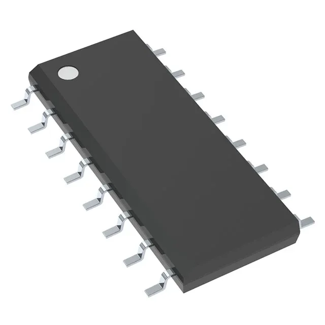
Texas Instruments CD74HC595M — Memory (DRAM / SRAM / Flash / EEPROM)

CD74HC595M 8-Bit Shift Register, 16-SOIC, 2V-6V

MPNCD74HC595M
End of Life

Texas Instruments 74HC series CD74HC595M is an 8-bit serial-in, parallel-out shift register with tri-state output latches. 16-SOIC package, 2V to 6V supply, -55°C to 125°C temperature range.

$1.31Ref. price · indicative, final on quote
Packaging16-SOIC (0.154", 3.90mm Width)
StockContact for availability
MOQ1 pcs
  • 100% new & originalTraceable channels only — no refurbs, no pulls, no remarked parts.
  • Date & lot codes on quoteStated per line before you commit; label photos on request.
  • MSL-compliant ESD packingMoisture-sealed bags with indicator cards; reels photo-verified.
  • PayPal buyer protectionPay by T/T, PayPal or Payoneer — card payments covered end to end.

Specifications

CD74HC595M Technical Specifications
ParameterValue
Series74HC
Logic typeShift Register
Output typeTri-State
Mounting typeSurface Mount
Voltage2V ~ 6V
Operating temperature-55°C ~ 125°C
PackageTube
FunctionSerial to Parallel, Serial
Case16-SOIC (0.154\", 3.90mm Width)
Number of elements1
Number of bits per element8

Product details

The CD74HC595M is an 8-bit serial-to-parallel shift register with a tri-state output latch, part of the 74HC series. It operates from 2V to 6V and over -55°C to 125°C.

The CD74HC595M is the industrial-temperature variant at -55°C to 125°C. Both parts cascade identically.

This part carries an Active lifecycle status and ROHS3 compliance. No end-of-life or last-time-buy notices are known.

Frequently asked questions

What is the difference between CD74HC595M and SN74HC595?

The CD74HC595M is rated for the full military temperature range of -55°C to 125°C, while the SN74HC595 is typically specified for commercial 0°C to 70°C. Both are 8-bit shift registers with tri-state outputs in 16-SOIC and share the same pinout and cascading logic.

What is the pinout of CD74HC595M?

Standard 16-SOIC pinout: Q1–Q7 on pins 1–7, GND pin 8, Q7S (serial out) pin 9, MR (reset) pin 10, SHCP (shift clock) pin 11, STCP (latch clock) pin 12, OE (output enable) pin 13, DS (data in) pin 14, Q0 pin 15, VCC pin 16.

How to cascade multiple CD74HC595M shift registers?

Connect Q7S (pin 9) of the first register to DS (pin 14) of the next. All SHCP (pin 11) and STCP (pin 12) pins share a common clock. Each additional register adds 8 parallel outputs. OE (pin 13) can be tied low for always-on outputs.

Can CD74HC595M be used with 5V Arduino?

Yes. The 2V to 6V supply range covers 5V operation directly. Connect VCC to 5V, GND to ground, and drive the SHCP, STCP, and DS pins with 5V logic from the Arduino. The tri-state outputs can drive LEDs, relays, or other 5V loads up to the 74HC output current limit.