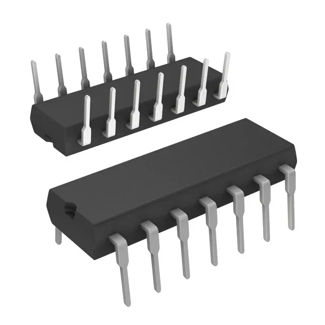
Quad NAND gate with Schmitt-trigger inputs — noise immunity for slow edges
The CD74HC132E is a Texas Instruments 74HC-series quad 2-input NAND gate with Schmitt-trigger inputs on all four gates. The hysteresis at the input — 0.3 V to 1.2 V low threshold vs 1.5 V to 4.2 V high threshold across the 2 V to 6 V supply range — cleans up slow or noisy edges that would cause a standard CMOS gate to oscillate or draw shoot-through current.
Quiescent current maxes at 2 µA — negligible in battery-powered or always-on logic. Each output sources or sinks 5.2 mA, enough to drive a standard LED through a 330-ohm resistor or fan out to four 74HC-series loads. Propagation delay is 21 ns at 6 V with a 50 pF load; at 4.5 V the delay stretches to roughly 30 ns, so budget the slower edge into the timing closure if the downstream device samples on the same clock edge.
Through-hole 14-DIP — board-fit and rework context
The 14-DIP (0.300-inch row spacing, 7.62 mm body width) is a through-hole package — the leads are 0.025-inch square on 0.100-inch pitch. No thermal pad, no exposed paddle. The hole-to-pad ratio for a standard 0.040-inch plated-through hole is generous, so hand-soldering or wave-solder is straightforward. The tube packaging means the leads are co-planar as shipped; no bake-out is required below MSL 1 for most rework profiles.
Active lifecycle and compliance — no obsolescence risk
The operating temperature range spans -55°C to 125°C, covering industrial and extended-temperature environments.