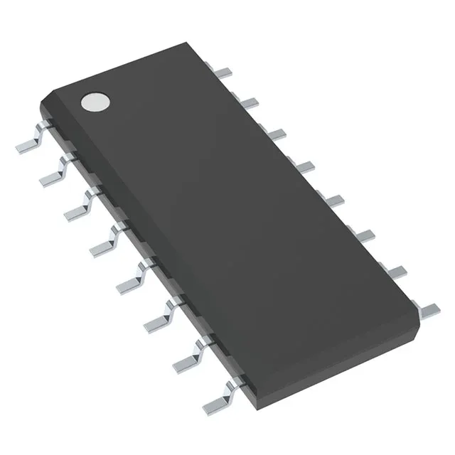
Timing, drive, and temperature envelope for design-in
The CD74AC112M96: Maximum propagation delay is 10.3 ns at 5V with a 50 pF load — this sets the timing budget for the clock-to-output path. In a 100 MHz chain, the 10 ns period leaves roughly 9.7 ns for the next stage after accounting for the flip-flop's own delay, so the fan-out and trace length must be managed to avoid setup-time violations. Each output sinks or sources 24 mA, enough to drive multiple standard-logic inputs or a small LED directly without a buffer. The quiescent current is 4 µA, so the part adds negligible standby draw in battery-powered equipment. A system deployed in an engine bay, satellite thermal-vacuum chamber, or arctic remote terminal can use this part without a separate temperature-grade variant. Input capacitance is 10 pF, typical for this logic family.