The CD4070BE: ROHS3 compliance is confirmed — the part contains no restricted substances under the EU RoHS directive, which covers most global markets including Europe, Asia-Pacific, and North America. No separate exemption paperwork is needed for new builds.
Wide supply range and temperature grade define the deployment envelope
The 3V to 18V supply span means this XOR gate works across legacy 5V TTL rails, 12V industrial buses, and 15V analog supplies without a separate level translator. A single CD4070BE can sit on a mixed-voltage backplane and still switch correctly as long as all inputs stay within the common-mode range. This qualifies the part for avionics, downhole instrumentation, engine-bay electronics, and outdoor telecom cabinets where the ambient swings beyond the commercial 0-70°C or industrial -40-85°C bands. A design targeting 105°C case temperature still has 20°C of margin before the absolute maximum. Quiescent current maxes at 1 µA across the full supply and temperature range. In a battery-backed circuit that spends most of its life in standby, the gate's own draw is below the self-discharge rate of a CR2032 coin cell — the system's sleep current is set by the MCU and the pull-up resistors, not this IC.
Logic function and timing — what the XOR does and how fast it gets there
Four independent 2-input XOR (Exclusive OR) gates in one 14-pin DIP. Each gate outputs a high when the two inputs differ — the fundamental building block for parity generators, digital comparators, and controlled inverters in data paths. The 4000B series uses a buffered output stage that gives symmetrical drive and noise immunity across the supply range. Propagation delay is 100 ns typical at 15V supply into a 50 pF load. This sets the maximum toggle rate at roughly 5 MHz for clean edge transitions — adequate for slow control signals, debounced switch inputs, and low-speed data buses, but not for high-frequency clock distribution or fast memory interfaces. The delay increases at lower supply voltages (roughly 250 ns at 5V), so a 3.3V rail design sees slower switching than a 12V one. Output drive capability is 3.4 mA source and sink at rated VOH/VOL. This drives one standard TTL load or up to four 4000B-series CMOS inputs directly, but it will not fan out to a heavy LED indicator or a long cable without a buffer stage. The input logic thresholds scale with supply: low level is 1.5V to 4V, high is 3.5V to 11V across the 3-18V range, so the gate interprets a 5V CMOS signal correctly even on a 12V supply rail.
Through-hole DIP — breadboard-friendly, legacy-compatible footprint
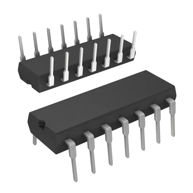
The 14-DIP (0.300" body width, 7.62 mm) through-hole package is the classic dual-inline format. It fits standard breadboards, perfboards, and 0.100-inch-pitch prototyping grids without an adapter. The 14-PDIP supplier device package designation confirms the plastic DIP variant — no ceramic side-brazed option here, so the temperature rating is achieved through the plastic molding compound, not hermetic sealing. Supplied in Tube packaging — 25 or 50 pieces per tube depending on the factory batch. For a repair bench or a low-volume production line, this avoids the reel fee and the tape-and-reel minimum order quantities that plague small-buyers on SMD parts. The tube also keeps the leads straight during storage, reducing the chance of bent pins during hand-insertion.