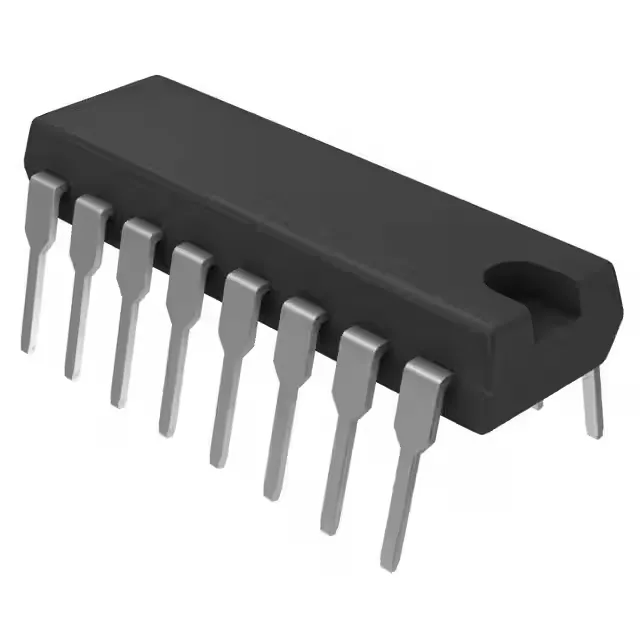
Six-channel inverter in the 4000B family
The CD4049UBE is a hex inverter from TI's 4000B series, packing six independent inverter gates in a single 16-pin DIP. Each gate has one input and one output, with the standard unbuffered topology that gives a clean transfer characteristic across the full supply range.
The 3V to 18V supply range is the headline spec for this part. At 5V it runs alongside TTL logic; at 12V or 15V it mates directly with industrial sensors, relays, and analog front-ends without level shifting. The input logic levels scale with VDD — low is 1V to 2.5V, high is 4V to 12.5V — so the thresholds track the rail. That means a 5V microcontroller can drive it, but a 3.3V logic output may not reach the high threshold unless VDD is dropped below 5V. The quiescent current maxes at 4 µA across the whole voltage range, so it adds negligible draw to a battery-backed or always-on rail.
Propagation delay and output drive
At 15V supply with a 50 pF load, the max propagation delay is 50 ns per gate. That is slow by modern 74AC or LVC standards, but it is more than adequate for switch debouncing, level translation, oscillator buffers, and control logic running below a few megahertz. The output can source 4.3 mA and sink 24 mA — enough to drive a standard LED or a low-power relay coil through a transistor, but not a heavy load directly. For high-speed clock trees or bus interfaces, look at the 74AC11004DW instead; for general-purpose industrial logic, this part is the workhorse.
Package and lifecycle — a through-hole staple
The CD4049UBE ships in a 16-pin DIP (0.300" body, 7.62 mm pitch) and is listed as Active with ROHS3 compliance. The through-hole package is a boon for prototyping, repair benches, and legacy board revs where a surface-mount swap would require a new PCB layout. Store the tubes in a dry, ESD-safe bin; the parts are MSL 1 (no bake needed before reflow if you wave-solder them), but the paper labels on the tubes can absorb humidity over years of shelf storage.