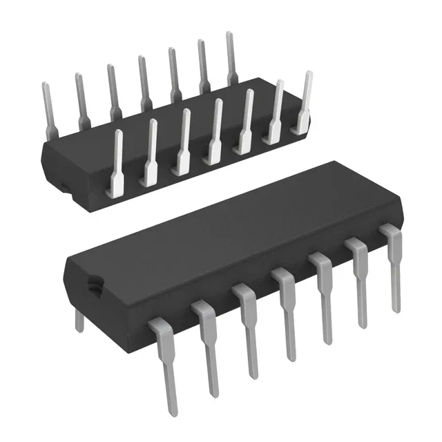
What the 3-input NOR buys you on a legacy or prototype board
The CD4025BE is a 4000B-series CMOS NOR gate packing three independent 3-input gates in a single 14-pin DIP — each gate outputs a logic high only when all three inputs are low, with the complementary truth table of a NAND. The 1 µA max quiescent current means it adds negligible static draw to a battery-backed or low-power rail, and the 3V to 18V supply range lets it run on the same unregulated rail as older 5V or 12V logic without a separate regulator. The 90 ns propagation delay at 15V and 50 pF load is typical of the 4000B family — adequate for control signals and slow-clock glue logic, but not for high-speed bus arbitration.
Through-hole DIP — board-fit and rework reality
The 14-DIP (0.300", 7.62mm) body with 0.100-inch pin pitch is a standard footprint that fits universal prototyping boards, wire-wrap panels, and legacy PCB layouts without a layout change. The 14-PDIP supplier package is the same mechanical outline — no hidden footprint variation between the two identifiers. For a surface-mount BOM line, the CD4025BM96 is the same die in an SOIC-14 package — same 3-input NOR function, same 3V–18V range and temperature grade — but the pinout shifts to a gull-wing footprint. A board laid out for the DIP cannot take the SOIC without a re-spin; the two are not drop-in interchangeable.
Temperature grade and supply flexibility
Input logic thresholds scale with VDD: low-level is 1.5V to 4V, high-level is 3.5V to 11V across the supply range. At 5V VDD, a 0.8V-low / 2.0V-high threshold is typical — compatible with 5V TTL and 3.3V CMOS if the 3.3V output high exceeds the 3.5V minimum. For 3.3V-only logic, a level shifter or a 74LVC gate is a safer fit.
Lifecycle and compliance — no PCN surprises
Because it is an active, widely second-sourced logic family, the supply risk is low. The BOM line can be dual-sourced with any compliant 4000B-series CD4025 from another qualified manufacturer — the JEDEC standard pinout and function are identical across vendors.