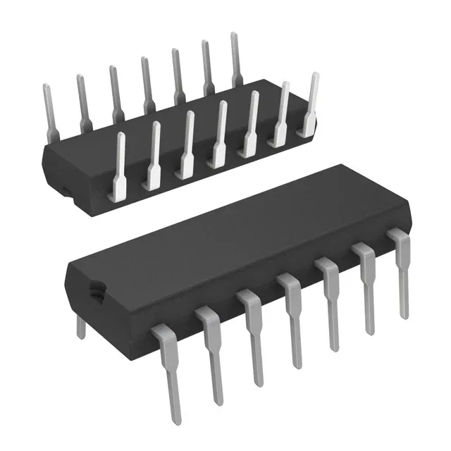
Quad 2-input NAND gate from the 4000B family
It operates across a 3V to 18V supply range and draws a maximum quiescent current of 1 µA, making it suitable for battery-powered or wide-supply-rail industrial logic where a 5V or 12V rail may droop.
Supply range and logic thresholds for mixed-voltage backplanes
The CD4011UBE accepts a 3V to 18V supply, which covers the common 5V and 12V logic rails used in industrial control panels, motor-drive interface boards, and telecom line cards. The input logic levels are specified as 1V to 2.5V for a low and 4V to 12.5V for a high, which means it can directly interface with older 5V TTL families or 12V-rated sensors without external level translation, as long as the high-level threshold is met.
Propagation delay and output drive at 15V
Maximum propagation delay is 50 ns at 15V supply with a 50 pF load. For a 5V supply the delay will be longer, typically around 125 ns, so timing closure in a 1 MHz clock tree is straightforward but a 10 MHz bus would need a faster family like 74HC. The 3.4 mA output current is symmetrical for both high and low states, which simplifies drive calculations for the downstream load.
Package and handling for the rework bench
The 14-DIP (0.300", 7.62mm) through-hole package is straightforward to hand-solder or wave-solder and fits standard 0.1-inch prototyping boards. No moisture sensitivity level (MSL) concern for a DIP — no bake-out required before assembly unless the parts have been stored in a humid environment for years. The 14-PDIP body is 19.3 mm long, suitable for socketing in test fixtures or field-replaceable modules.
Sourcing posture for this BOM line
The active lifecycle status means there is no imminent last-time-buy pressure, so the BOM line can be committed for production without a short-term LTB risk.