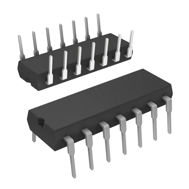
Active production, through-hole CMOS NAND gate
Packaged in a 14-pin DIP (0.300", 7.62mm) for through-hole mounting, it is a direct fit for breadboard prototyping, legacy system repairs, or new designs that require the wide supply tolerance and low static power of the 4000B family.
The 3V to 18V supply range is the defining feature of the 4000B series. It allows the CD4011BE to interface directly with 5V TTL, 12V industrial rails, or 3.3V battery systems without a level translator. The input logic thresholds scale with VDD: low-level thresholds run from 1.5V to 4V, and high-level thresholds from 3.5V to 11V, ensuring consistent noise margins across the supply range.
The 125°C upper limit covers under-hood automotive applications, though note this part is not AEC-Q100 qualified — for automotive-grade CMOS NAND gates, look to the CD74HC or CD74HCT series with AEC-Q certification.
Through-hole 14-DIP: prototyping and rework friendly
The 14-DIP (0.300", 7.62mm) package with 0.1" pin spacing is the standard through-hole footprint. It is ideal for hand-assembled prototypes, socketed test boards, or field repairs where a surface-mount part would be impractical. The through-hole body also tolerates multiple soldering/desoldering cycles better than a fine-pitch SMD package, making it a good choice for development iterations or legacy system maintenance.
Propagation delay: 90 ns at 15V, 50 pF
Maximum propagation delay is 90 ns with a 15V supply and 50 pF load. This is slower than 74HC or 74HCT family gates (typically 10–30 ns), so the CD4011BE is not a fit for high-speed clock distribution or fast data paths. It is well suited for control logic, debounce circuits, oscillator gates, or any application where the signal rate stays below a few megahertz and the wide supply range or low quiescent current is the priority.
Output drive: 3.4 mA source and sink
This is sufficient to drive a single TTL load, an LED with a series resistor, or the input of another CMOS gate. For heavier loads — relays, high-current LEDs, or long cables — buffer the output with a transistor or a dedicated driver IC. The symmetrical drive simplifies interface design: the same resistor value works for both high and low states.
For dual-sourcing or supply-chain resilience, the 4000B series includes functionally similar NAND gates such as the CD4011B in other package variants, but the CD4011BE is the through-hole DIP version.