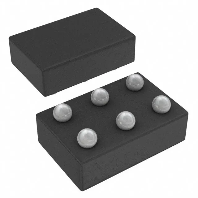
The BQ25100AYFPR: Battery regulation voltage is 4.3 V, slightly above the standard 4.2 V Li-ion termination. This gives about 2% more capacity per cycle at the cost of slightly accelerated calendar aging — a trade-off TI targets at devices where runtime trumps cycle life. The 6.45 V absolute maximum supply input means the part survives a 5 V USB rail with margin, but a 5.5 V adapter is the practical ceiling before the over-voltage protection trips.
Package and board-fit — the DSBGA footprint reality
The tiny footprint — roughly 1.2 mm × 0.9 mm — fits behind a USB connector on a wearable PCB, but the exposed thermal pad area is minimal. Layout must route the charge current path with short, wide traces to keep the junction temperature below the 125°C ceiling at full 250 mA charge from a 5 V rail. Surface-mount only — no through-hole variant exists. The 6-DSBGA supplier device package is the same physical footprint as the base product number BQ25100, so a single PCB land pattern serves the whole family if you need to swap between fixed-voltage versions.
Protection features — what shuts the charger down
Three fault protections are built in: over-temperature (die-level thermal shutdown, typically 150°C), over-voltage on the input pin, and output short-circuit. No external watchdog or supervisor IC is needed for safe charging — the part self-limits. The only programmable feature is the charge current; there is no I2C interface, no timer, and no battery-temperature sense input. For designs that need NTC monitoring, a companion part in the BQ25100 family adds that pin.