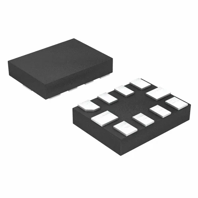
Active SAR ADC with I²C — 140k SPS, 12-bit, 2-channel
The ADS7142IRUGR is a 12-bit successive-approximation-register (SAR) ADC from Texas Instruments, sampling at 140k samples per second over an I²C bus. Its two input channels are configurable as pseudo-differential or single-ended, and the internal multiplexer routes them into a single SAR core — no external mux needed for dual-channel applications.
140k SPS over I²C — bus timing and throughput
At 140k SPS, each conversion completes in roughly 7 µs. Over a 400 kHz I²C bus, the read-back transaction adds about 5–6 µs, so the aggregate per-channel throughput stays above 60k SPS in continuous mode. The 0:1 S/H-to-ADC ratio means there is no sample-and-hold — the SAR core samples the input directly on the conversion start, which simplifies the drive requirement but demands a low-impedance source to settle within the acquisition window.
Supply-referenced architecture — no external reference needed
The reference type is the supply rail itself, so the ADC's full-scale range tracks the analog supply voltage. A 3.3 V supply gives a 0–3.3 V input span; a 1.8 V supply gives 0–1.8 V. This eliminates the external reference IC and its bypass capacitors, saving board area — useful in space-constrained designs like the 10-X2QFN (2x1.5 mm) package.
The 10-pin X2QFN (2x1.5 mm) package has a 0.5 mm pitch — hand-solderable with a fine tip and flux, but a hot-air rework station is recommended for consistent wetting on the centre pad.