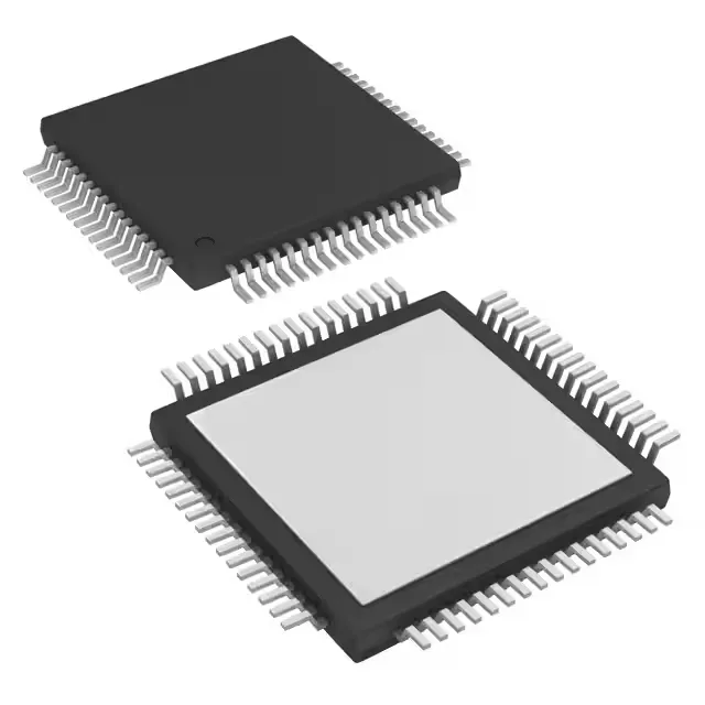
64-pin HTQFP — what the package demands of the board
The ADS1274IPAPT ships in a 64-PowerTQFP package, also specified as the supplier device package 64-HTQFP (10x10 mm). The 0.5 mm pin pitch demands a controlled-impedance layout for the SPI bus lines, especially at the 144 kSPS conversion rate where digital switching noise can couple into the analog supply.
Four simultaneous 24-bit sigma-delta converters — what the 144 kSPS means
The ADS1274 integrates four independent 24-bit sigma-delta ADCs, each with a differential input. The sampling rate of 144 kSPS per second applies per converter — all four channels can simultaneously sample at that rate, giving an aggregate throughput of 576 kSPS. The sigma-delta architecture inherently oversamples and digital-filters the input, so the effective data rate at the SPI output is lower than the modulator rate; the 144 kSPS figure is the output data rate after decimation. The differential input structure rejects common-mode noise on the analog front-end, which is critical when the ADC is reading bridge sensors, thermocouples, or shunt resistors in a noisy industrial environment. The reference is external, so the converter's accuracy depends on the reference voltage source and its temperature drift.
Dual supply rails and SPI interface
The analog supply is fixed at 5 V, while the digital supply accepts 1.65 V to 1.95 V. This dual-supply architecture lets the digital I/O operate at a lower voltage (e.g., 1.8 V) to interface directly with a low-voltage FPGA or MCU without an external level shifter. The SPI data interface handles the conversion results and configuration register access. The part is ROHS3 compliant per Texas Instruments' standard lead-free plating.