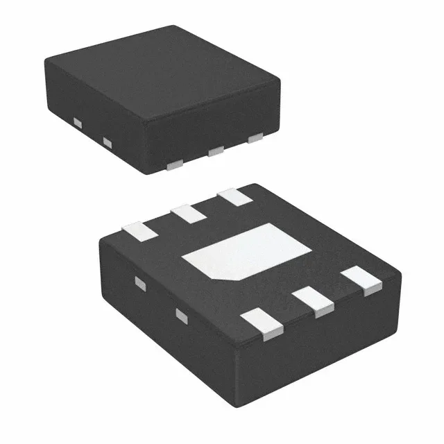
10-bit SAR ADC in a 6-WSON — what the 200 kSPS and single supply mean for your BOM
The ADC101S021CISD/NOPB is a 10-bit successive-approximation-register (SAR) ADC from Texas Instruments, sampling at 200 kSPS with a single-ended input. The SAR architecture means the conversion is deterministic — no pipeline delay — so the sample timing is predictable cycle-to-cycle, which matters when the ADC is triggered by a timer or PWM edge in a motor-drive or sensor-loop application. This simplifies the power tree and reduces BOM count, but it also means the ADC's full-scale range tracks the supply voltage: a 3.3 V rail gives a 0–3.3 V input span, and any supply noise couples directly into the conversion result. The SPI/DSP serial interface connects directly to most MCU SPI peripherals with a single data line, a clock, and a chip-select. The conversion is initiated by the chip-select edge, and the 10-bit result is shifted out on the next 10–16 SCLK cycles — no external start-convert pin needed.
Package, footprint, and thermal — the 6-WSON exposed pad
The exposed pad on the bottom must be soldered to a PCB thermal land and connected to the analog ground plane — this is the primary thermal path and also the electrical ground reference for the ADC. Without a proper via array under the pad, the junction temperature rises above the 85 °C ambient limit faster than the 0.5 °C/W thermal resistance suggests.